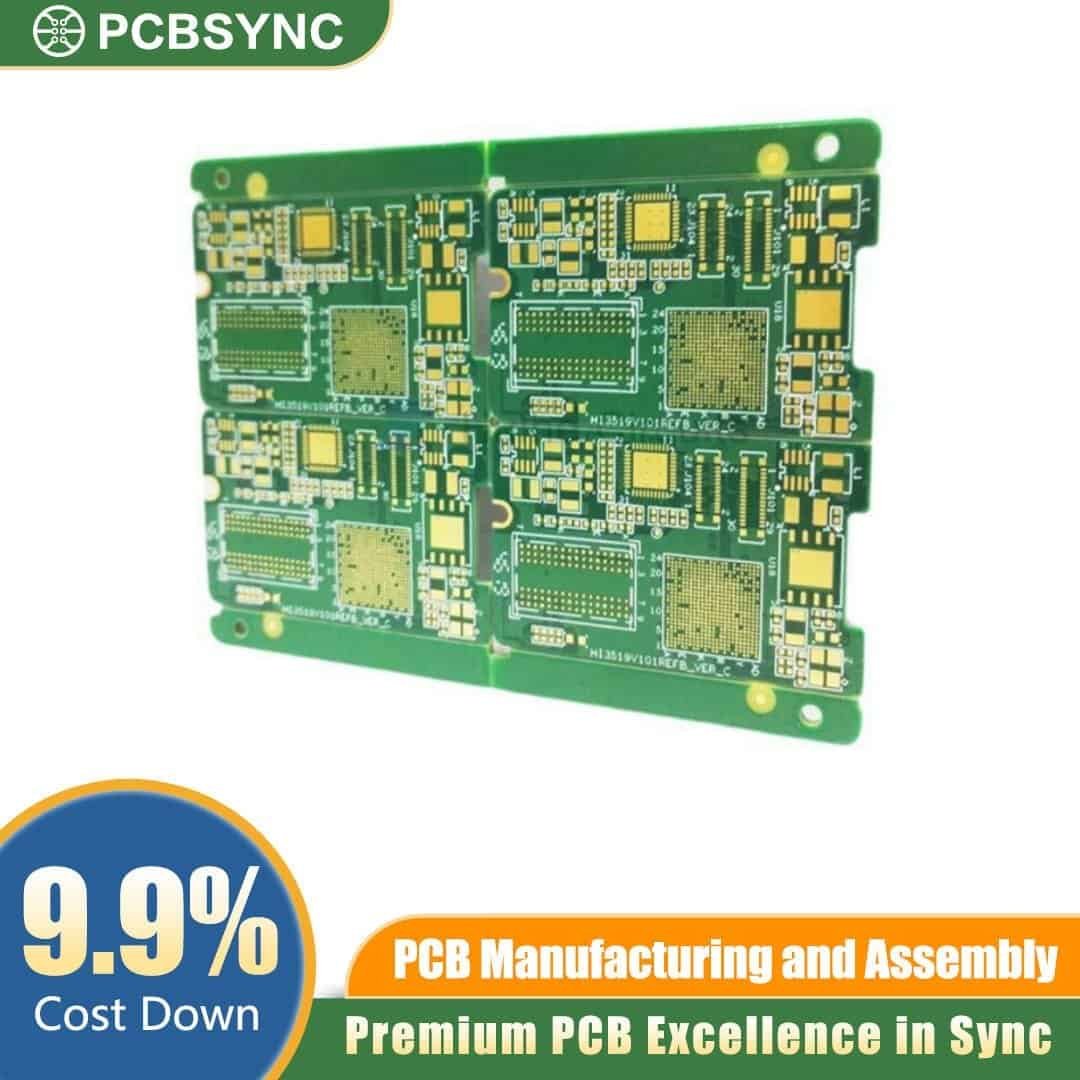
For design engineers facing strict spatial constraints, the Stacked Blind Via HDI PCB provides essential vertical layer connection capabilities. By stacking laser-drilled blind vias directly above one another, this HDI PCB structure minimises layer transition area, improves signal integrity, and supports the extreme component densities required in modern microelectronics. This architecture is vital for procurement teams and product developers constructing multi-layered circuits where staggered vias consume excessive surface space.
-
Via Architecture: Copper-filled stacked blind vias and microvias for direct vertical routing.
-
Layer Count: Configurable for complex multi-layer designs (typically 4 to 24+ layers).
-
Materials: FR4, Rogers, Polyimide, or high-TG dielectrics for controlled impedance.
-
Aspect Ratio: Precision laser drilling with optimised via-to-pad ratios for reliability.
-
Standards Compliance: Manufactured to strict IPC-6012 Class 2 and Class 3 specifications.
-
Telecommunications: 5G infrastructure, high-speed networking switches, and routers.
-
Medical Devices: Portable diagnostic equipment, imaging machinery, and wearable health monitors.
-
Aerospace & Defence: Radar modules, avionics control systems, and satellite communication links.
-
Consumer Electronics: Advanced mobile devices and compact computing hardware.
PCBSYNC is a professional PCB fabrication, PCBA, and EMS manufacturer delivering precision-built electronics for aerospace, medical, automotive, industrial, and smart energy applications. We handle everything from rapid prototyping to mass production — including rigid, flexible, and rigid-flex PCBs, full turnkey assembly, component sourcing, AOI and X-ray inspection, and OEM/ODM support. Reliable boards. Consistent quality. From prototype to production — PCBSYNC.
Optimise your next electronic design with advanced vertical interconnection. Request a quote or contact our engineering team today to discuss your specific fabrication requirements.