Contact Sales & After-Sales Service

Contact & Quotation

  • Inquire: Call 0086-755-23203480, or reach out via the form below/your sales contact to discuss our design, manufacturing, and assembly capabilities.
  • Quote: Email your PCB files to Sales@pcbsync.com (Preferred for large files) or submit online. We will contact you promptly. Please ensure your email is correct.
Drag & Drop Files, Choose Files to Upload You can upload up to 3 files.

Notes:
For PCB fabrication, we require PCB design file in Gerber RS-274X format (most preferred), *.PCB/DDB (Protel, inform your program version) format or *.BRD (Eagle) format. For PCB assembly, we require PCB design file in above mentioned format, drilling file and BOM. Click to download BOM template To avoid file missing, please include all files into one folder and compress it into .zip or .rar format.

Electronic Components Sourcing

Sourcing high-quality electronic components is essential to create quality products for your brand. Choosing the right parts ensures that your products are functional and useful for end users.

Our prototype runs are often a mix of large BGAs and tiny 0201 components, and we’ve had issues with other assembers on yield. PCBsync’s assembly team delivered a perfect first-run success. The board was pristine, the solder joints were impeccable under the microscope, and everything worked straight out of the box. Their attention to detail in the assembly process saved us weeks of debug time. They are now our go-to for critical prototype assembly.

Scaling from hundreds to tens of thousands of units for our smart home device presented huge supply chain and manufacturing challenges. PCBsync’s full electronic manufacturing service was the solution. They didn’t just build the PCB; they managed the entire box-build, sourced all components (even during shortages), and implemented a rigorous quality control system that drastically reduced our field failure rate. They act as a true extension of our own production team.

2+N+2 HDI PCB Stackup – Dual Build-Up Microvia Board

Product Details

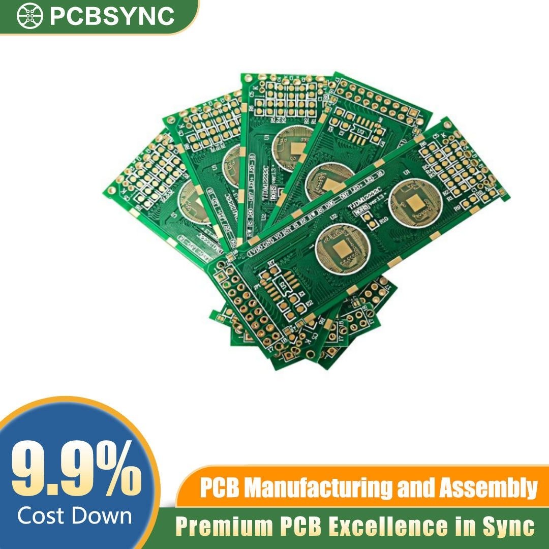
The 2+N+2 HDI PCB Stackup delivers the advanced architecture required for next-generation, high-density digital designs. By utilizing a dual-layer sequential build-up (SBU) process, this board integrates two layers of laser-drilled microvias on both the top and bottom surfaces of a central core ( layers). This specific layout dramatically increases routing density, allowing hardware developers to successfully route ultra-fine pitch BGAs down to 0.4 mm while reducing overall layer count and minimizing signal attenuation.

Key Features of 2+N+2 HDI PCB Technology

  • Dual-Layer Microvias: Supports stacked, staggered, skip, and copper-filled via-in-pad structures for maximum routing efficiency.

  • Controlled Impedance: Advanced dielectric materials and tight manufacturing tolerances ensure stable differential and single-ended signaling.

  • Fine Line and Space: Capable of trace widths and spacing down to 3 mil () for high-speed routing.

  • Premium Substrates: Available in high- FR-4, halogen-free, and low-loss materials to maintain thermal and structural stability.

  • Surface Finishes: ENIG, ENEPIG, or OSP options available to ensure excellent solderability and reliable component joints.

Applications

  • Telecommunications: High-speed routers, 5G wireless network infrastructure, and RF switching equipment.

  • Computing and Storage: Compact single-board computers (SBCs), high-performance servers, and memory modules.

  • Consumer Electronics: Premium smartphones, wearable technology, and ultra-thin IoT devices.

  • Industrial Automation: High-reliability control units, advanced sensor hubs, and robotics modules.

Why Choose PCBSYNC

PCBSYNC is a professional PCB fabrication, PCBA, and EMS manufacturer delivering precision-built electronics for aerospace, medical, automotive, industrial, and smart energy applications. We handle everything from rapid prototyping to mass production — including rigid, flexible, and rigid-flex PCBs, full turnkey assembly, component sourcing, AOI and X-ray inspection, and OEM/ODM support. Reliable boards. Consistent quality. From prototype to production — PCBSYNC.

Ready to take your high-density interconnect design from layout to reality? Contact the engineering team at PCBSYNC today to discuss your technical specifications or to submit your Gerber files for a detailed quote.

Contact Sales & After-Sales Service

Contact & Quotation

  • Inquire: Call 0086-755-23203480, or reach out via the form below/your sales contact to discuss our design, manufacturing, and assembly capabilities.

  • Quote: Email your PCB files to Sales@pcbsync.com (Preferred for large files) or submit online. We will contact you promptly. Please ensure your email is correct.

Drag & Drop Files, Choose Files to Upload You can upload up to 3 files.

Notes:
For PCB fabrication, we require PCB design file in Gerber RS-274X format (most preferred), *.PCB/DDB (Protel, inform your program version) format or *.BRD (Eagle) format. For PCB assembly, we require PCB design file in above mentioned format, drilling file and BOM. Click to download BOM template To avoid file missing, please include all files into one folder and compress it into .zip or .rar format.