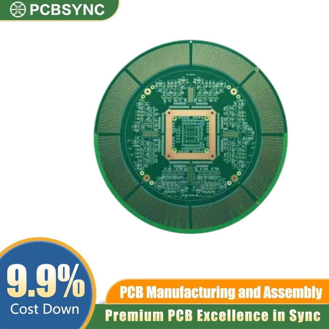
When space constraints meet high-pin-count components, engineers require advanced interconnect solutions. The laser-drilled blind via HDI PCB provides the routing density necessary for modern electronics. By utilising precision microvia technology, these boards allow for complex layer transitions without consuming valuable surface area, ensuring electrical performance and signal integrity for critical product developments.
-
Microvia Diameter: Precision laser-drilled vias down to 3 mil (75 µm) for dense routing.
-
Layer Count: Configurable up to 24 layers, supporting any-layer HDI structures.
-
Material Compatibility: Engineered with FR4, Rogers, and Megtron laminates for controlled impedance requirements.
-
Blind and Buried Vias: Sequential build-up (SBU) technology maximises space utilisation.
-
Surface Finish: Available in ENIG, ENEPIG, and Immersion Silver for optimal component soldering.
-
Compliance: Manufactured to IPC-6012 Class 2 and Class 3 standards.
This microvia interconnect technology serves industries demanding miniaturisation and reliability:
-
Telecommunications: 5G infrastructure, routers, and high-speed network switches.
-
Medical Devices: Wearable monitors, diagnostic imaging equipment, and implantable technology.
-
Aerospace & Defence: Radar systems, avionics, and secure communication modules.
-
Automotive: Advanced Driver Assistance Systems (ADAS) and EV control units.
PCBSYNC is a professional PCB fabrication, PCBA, and EMS manufacturer delivering precision-built electronics for aerospace, medical, automotive, industrial, and smart energy applications. We handle everything from rapid prototyping to mass production — including rigid, flexible, and rigid-flex PCBs, full turnkey assembly, component sourcing, AOI and X-ray inspection, and OEM/ODM support. Reliable boards. Consistent quality. From prototype to production — PCBSYNC.
Ready to integrate advanced microvia structures into your next design? Request a quote from our engineering team to discuss your specific manufacturing requirements.