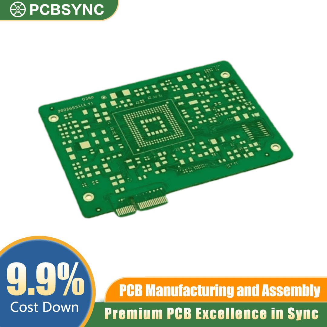
The Copper-Filled Buried Via HDI PCB is engineered to handle the intense routing density and demanding thermal profiles of next-generation electronics. By utilizing a via-in-pad core filled with solid copper, this board facilitates efficient heat dissipation and robust electrical conductivity directly beneath surface-mount components. It provides design engineers and procurement managers with the structural reliability needed to prevent signal degradation in tight, multi-layered layouts.
Key Features of Copper-Filled Buried Via HDI PCB
-
Via-in-Pad Core Technology: Maximizes routing space by placing vias directly under component land pads, filled completely with electroplated copper.
-
Advanced Material Options: Fabricated using high-Tg FR-4, halogen-free materials, or high-speed low-loss laminates (e.g., Rogers, Isola).
-
Precise Microvia Geometry: Supports laser-drilled blind and buried microvias with aspect ratios optimized for signal integrity.
-
Fine Line and Space: Capable of linewidths and spacings down to 50 µm to accommodate ultra-fine pitch BGA components.
-
Surface Finishes: Available in ENIG, ENEPIG, or Immersion Silver for optimal solderability and coplanarity.
-
Compliance Standards: Manufactured in accordance with IPC-A-600 Class 2 or Class 3 specifications, RoHS, and REACH.
Applications
-
Telecommunications: High-speed routers, 5G base stations, and optical networking modules.
-
Computing & Storage: High-density servers, memory modules, and multi-core processing units.
-
Aerospace & Defence: Compact avionics guidance systems and ruggedized communication payloads.
-
Medical Devices: High-resolution imaging systems and implantable monitoring equipment.
Why Choose PCBSYNC
PCBSYNC is a professional PCB fabrication, PCBA, and EMS manufacturer delivering precision-built electronics for aerospace, medical, automotive, industrial, and smart energy applications. We handle everything from rapid prototyping to mass production — including rigid, flexible, and rigid-flex PCBs, full turnkey assembly, component sourcing, AOI and X-ray inspection, and OEM/ODM support. Reliable boards. Consistent quality. From prototype to production — PCBSYNC.
Ready to take your high-density project to the next level? Contact our technical engineering team today to review your Gerber files, discuss stack-up configurations, or request a comprehensive quote.