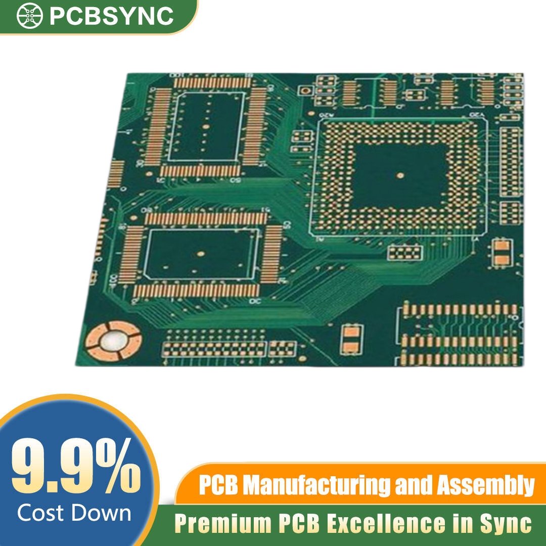
8-Layer Buried Via HDI PCB Overview
This HDI PCB provides an advanced substrate for engineers requiring highly integrated circuitry. The 8-Layer Buried Via HDI PCB functions as a dense core multilayer framework, optimising space utilisation while maintaining strict signal integrity. Procurement managers and product developers specify this architecture when facing stringent form-factor constraints in modern electronic devices.
Key Features
-
Buried Via Architecture: Facilitates internal layer connections without occupying surface space.
-
Layer Stackup: 8-layer configuration for segregated power, ground, and multiple signal routing planes.
-
Routing Density: Dense core multilayer construction accommodates fine-pitch BGA components.
-
Advanced Materials: FR4 TG170 or equivalent laminates ensuring thermal stability under operational stress.
-
Manufacturing Standards: IPC-A-600 Class 2 or Class 3 compliance for industrial reliability.
Applications
This board architecture is deployed across sectors demanding compact, precision-built hardware.
-
Telecommunications: Networking switches and compact routers requiring robust signal layers.
-
Medical Devices: Portable diagnostics and wearable monitors necessitating miniaturisation.
-
Aerospace: Avionics modules where weight reduction and structural integrity remain critical.
-
Industrial Controls: Compact sensor nodes and complex automation controllers.
Why Choose PCBSYNC
PCBSYNC is a professional PCB fabrication, PCBA, and EMS manufacturer delivering precision-built electronics for aerospace, medical, automotive, industrial, and smart energy applications. We handle everything from rapid prototyping to mass production — including rigid, flexible, and rigid-flex PCBs, full turnkey assembly, component sourcing, AOI and X-ray inspection, and OEM/ODM support. Reliable boards. Consistent quality. From prototype to production — PCBSYNC.
Ready to advance your next hardware project? Request a comprehensive quote today to discuss your exact specifications.