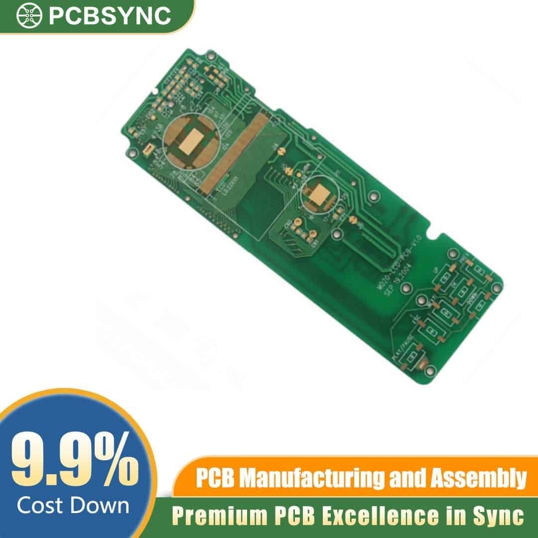
The Resin-Filled Blind Via HDI PCB delivers advanced routing capabilities for complex electronic designs. By filling blind vias with premium epoxy resin and applying protected plating over the surface, engineers achieve a flat, solderable finish essential for via-in-pad placements. This structural approach minimises signal loss, enhances thermal dissipation, and supports the dense component packaging required in modern smart devices, instrumentation, and hardware.
Key Features of our Resin-Filled Blind Via HDI PCB
-
Via-in-Pad Compatibility: Resin filling combined with protected surface plating creates a coplanar surface, preventing solder wicking during assembly.
-
Microvia Structures: Engineered to support fine-pitch BGA components and dense routing requirements.
-
Controlled Impedance: Precise layer stack-ups and trace widths ensure accurate high-speed signal transmission.
-
Material Versatility: Available in standard FR4, high-TG, and halogen-free laminates to meet strict thermal and environmental standards.
-
Enhanced Reliability: Plating over filled vias protects against moisture ingress and thermal expansion stresses.
Applications
-
Medical diagnostics and portable imaging equipment.
-
Aerospace navigation and compact communication modules.
-
High-speed telecommunications infrastructure.
-
Industrial automation and sensory control systems.
Why Choose PCBSYNC
PCBSYNC is a professional PCB fabrication, PCBA, and EMS manufacturer delivering precision-built electronics for aerospace, medical, automotive, industrial, and smart energy applications. We handle everything from rapid prototyping to mass production — including rigid, flexible, and rigid-flex PCBs, full turnkey assembly, component sourcing, AOI and X-ray inspection, and OEM/ODM support. Reliable boards. Consistent quality. From prototype to production — PCBSYNC.
Discuss your specific board requirements with our engineering team or request a quote for your next manufacturing run.