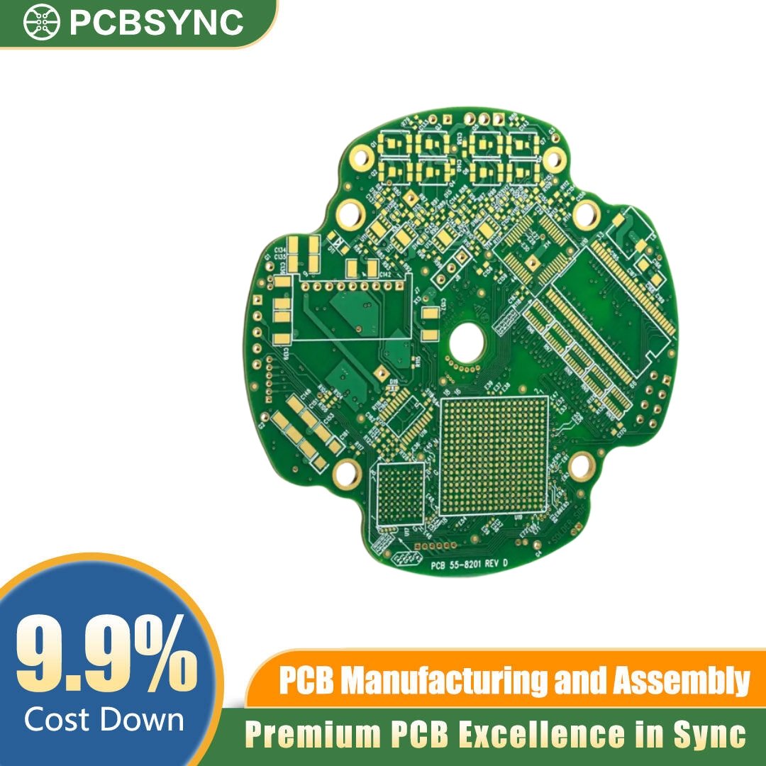
When developing next-generation mobile devices, electronics engineers require a Smartphone HDI PCB that enables complex routing within highly constrained spatial parameters. This any-layer microvia mainboard provides the structural integrity and electrical performance necessary for cellular technology, 5G communications, and advanced mobile processing units. By utilising stacked and staggered microvias, hardware developers can minimise board size while increasing component density and maintaining stringent signal transmission requirements.
-
Any-Layer Microvia Architecture: Facilitates blind and buried routing between any layers for maximum spatial efficiency.
-
Specialised Material Selection: Constructed using FR-4 and high-Tg dielectrics engineered to withstand thermal stress during extended operation.
-
Impedance Control: Strict tolerance management ensures reliable high-frequency signal integrity across RF and digital traces.
-
Fine Pitch Routing: Supports the tight trace-to-trace spacing required for dense BGA (Ball Grid Array) component integration.
-
Manufacturing Standards: Fabricated to meet IPC Class 2 and IPC Class 3 specifications for mission-critical reliability.
-
Flagship and mid-tier smartphones
-
Wearable telecommunication devices
-
Compact internet-connected (IoT) equipment
-
Portable medical diagnostic instruments
PCBSYNC is a professional PCB fabrication, PCBA, and EMS manufacturer delivering precision-built electronics for aerospace, medical, automotive, industrial, and smart energy applications. We handle everything from rapid prototyping to mass production — including rigid, flexible, and rigid-flex PCBs, full turnkey assembly, component sourcing, AOI and X-ray inspection, and OEM/ODM support. Reliable boards. Consistent quality. From prototype to production — PCBSYNC.
Submit your Gerber files today to request a quote and review custom manufacturing parameters with our engineering team.