Inquire: Call 0086-755-23203480, or reach out via the form below/your sales contact to discuss our design, manufacturing, and assembly capabilities.
Quote: Email your PCB files to Sales@pcbsync.com (Preferred for large files) or submit online. We will contact you promptly. Please ensure your email is correct.
Notes: For PCB fabrication, we require PCB design file in Gerber RS-274X format (most preferred), *.PCB/DDB (Protel, inform your program version) format or *.BRD (Eagle) format. For PCB assembly, we require PCB design file in above mentioned format, drilling file and BOM. Click to download BOM template To avoid file missing, please include all files into one folder and compress it into .zip or .rar format.
If your design is hitting a thermal wall, arcing under high voltage, or losing signal integrity at GHz frequencies, an alumina PCB is probably already on your shortlist. This guide walks through what alumina ceramic substrates actually are, the specs that matter, the manufacturing routes (DPC, DBC, thick film, thin film), and where they outperform — or lose to — FR4 and aluminum nitride.
You will leave with a clear decision framework for when to specify alumina, what purity grade to ask for, and the questions to put to your supplier before you cut a PO.
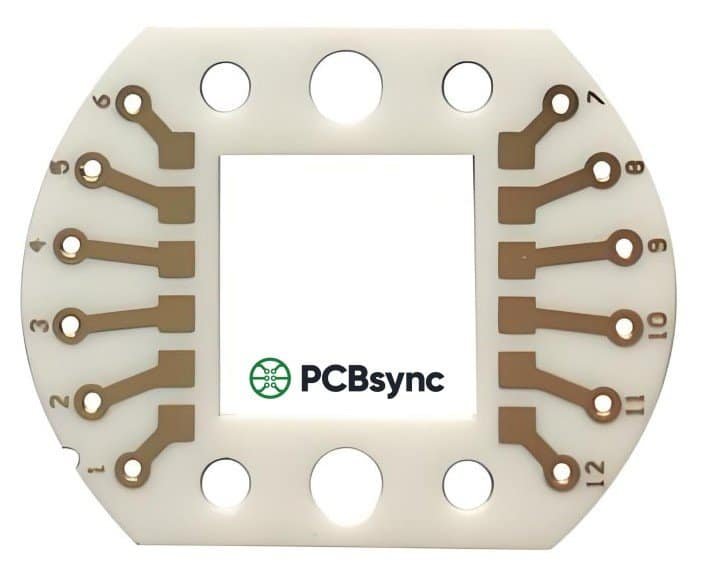
An alumina PCB is a printed circuit board built on a ceramic substrate of aluminum oxide (Al₂O₃) instead of the glass-reinforced epoxy used in FR4. The ceramic base gives the board high thermal conductivity, excellent electrical insulation, and dimensional stability at temperatures that would delaminate a standard PCB.
Alumina substrates typically come in purity grades of 92%, 96%, and 99.6%. Higher purity means better thermal performance and lower dielectric loss, but also higher cost and harder machining. The 96% grade is the workhorse of the industry — it balances cost and performance for the majority of LED, power, and RF applications.
How It Differs from FR4 and Metal-Core PCBs
FR4 is cheap, easy to drill, and works fine below about 130 °C — but its thermal conductivity is roughly 0.3 W/m·K. A metal-core PCB (MCPCB) bumps that to around 1–3 W/m·K through an aluminum baseplate, but the dielectric layer is still polymer. An alumina PCB skips the polymer entirely and conducts heat through ceramic, reaching 24–28 W/m·K. That’s roughly 80× better than FR4.
Key Specifications That Matter
Spec sheets vary by manufacturer, but the values below are typical for the 96% and 99.6% alumina grades you will see from reputable fabricators.
Property
96% Alumina
99.6% Alumina
FR4 (reference)
Thermal conductivity (W/m·K)
24
28–30
0.3
Dielectric constant @ 1 MHz
9.4
9.8
4.5
Dielectric loss (tan δ)
0.0004
0.0001
0.02
CTE (ppm/°C, 25–300 °C)
7.2
7.4
14–17
Flexural strength (MPa)
320
380
—
Max operating temp (°C)
350+
350+
~130
Volume resistivity (Ω·cm)
10¹⁴
10¹⁴
10¹⁰
Two numbers do most of the heavy lifting in design decisions: thermal conductivity and CTE. Alumina’s CTE of ~7 ppm/°C sits much closer to silicon (~3 ppm/°C) than FR4 does, which means die-attached components experience less thermal stress over temperature cycles — a big deal for reliability in automotive and aerospace work.
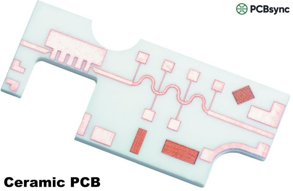
How Alumina PCBs Are Manufactured
“Alumina PCB” is a substrate choice, not a single process. The copper conductor pattern can be applied in four very different ways, and each has its own cost, line/space capability, and current-carrying limits.
Thick Film (TF)
Conductive paste — usually silver, silver-palladium, or gold — is screen-printed onto the fired alumina, then re-fired at around 850 °C. Thick film is the lowest-cost route and dominates simple LED and resistor-heater work. Minimum line/space is typically 100/100 µm.
Thin Film
Metals are vacuum-sputtered onto polished alumina, then photolithographically etched. Thin film delivers extremely tight tolerances (line/space down to 20/20 µm) and clean RF behavior, but it is the most expensive process. Use it for microwave circuits, sensors, and precision attenuators.
DPC (Direct Plated Copper)
A thin seed layer is sputtered onto the ceramic, then electroplated copper is built up and patterned. DPC alumina PCBs are the modern default for high-power LEDs and laser diodes: thermal vias are easy to fill, line/space can reach 50/50 µm, and copper thickness scales from a few microns up to 150 µm.
DBC (Direct Bonded Copper)
Thick copper foil (typically 0.2–0.6 mm) is bonded directly to the alumina at around 1065 °C via a eutectic reaction. DBC substrates are the standard for IGBT and SiC power modules where currents run from tens to hundreds of amps. They cannot match DPC’s fine-line resolution, but they handle the heat.
Where Alumina PCBs Win — and Where They Don’t
Alumina is not a universal upgrade. It is brittle, heavier than FR4, harder to drill (you need laser or diamond tools), and more expensive per square inch. The decision comes down to whether your design genuinely needs what ceramic offers.
Use alumina when you need to dissipate >3 W/cm² of heat, operate above 150 °C, hold tight CTE to silicon, run at GHz frequencies with low loss, or guarantee 10+ year reliability under thermal cycling.
Avoid alumina when the board needs to flex, mechanical shock is severe (drop tests on consumer gear), the design has hundreds of through-holes, or unit cost is the dominant constraint.
Alumina vs. Aluminum Nitride (AlN)
Aluminum nitride is the next step up — thermal conductivity of 170–230 W/m·K, roughly 7× better than alumina. It also tracks silicon’s CTE more closely (~4.5 ppm/°C). The catch is price: AlN substrates typically run 3–5× the cost of comparable alumina, and the supply base is narrower. Specify AlN only when alumina cannot move the heat fast enough — usually above ~30 W/cm² heat flux, or in SiC/GaN power modules where junction temperatures exceed 175 °C.
Top Applications for Alumina PCBs
Across the industries we see most often in production, alumina earns its keep in a handful of repeating use cases.
High-power LED lighting — automotive headlamps, stadium floods, UV-C disinfection modules, and horticultural grow lights all push heat fluxes that polymer dielectrics simply cannot handle long-term.
Power electronics — DBC alumina substrates remain the volume choice for industrial IGBT modules, EV traction inverters in the lower-power tiers, and solar inverters.
RF and microwave — thin-film alumina is standard for satellite communication filters, radar front-ends, and 5G/6G test equipment thanks to its low loss tangent and tight tolerances.
Automotive electronics — engine control modules, transmission sensors, and ignition systems live in 150 °C+ underhood environments where FR4 ages out fast.
Medical and aerospace — implantable device hybrids, MRI gradient amplifiers, and avionics modules use alumina for its biocompatibility, hermeticity, and radiation tolerance.
Industry guidance from the IPC standards body (ipc.org) covers ceramic substrate inspection, qualification, and reliability testing in detail — worth pulling before you finalize a spec.
How to Specify an Alumina PCB Without Costly Mistakes
Most failed alumina projects we audit go wrong at the RFQ stage, not at the fab. Send your supplier a drawing that answers all of the following, and you will get sharper quotes and fewer surprises:
Substrate grade and thickness: 96% vs 99.6%, and 0.25 / 0.38 / 0.635 / 1.0 mm — thinner means better thermal transfer but more fragile handling.
Process: thick film, thin film, DPC, or DBC — the right answer depends on current, line/space, and budget.
Copper thickness: typical ranges run 18–150 µm for DPC and 200–600 µm for DBC.
Surface finish: ENIG, ENEPIG, immersion silver, or gold wire-bondable plating for die attach.
Hole strategy: laser-drilled vias for DPC, mechanical drilled holes only on thicker substrates — and budget for slow drill speeds.
Edge profile: laser cut, scribe-and-break, or full machined edges — this drives both cost and edge strength.
One practical tip: alumina ships with a “rough” as-fired surface (~0.5 µm Ra) or a polished surface (<0.1 µm Ra). Thin-film RF designs need polished; thick-film LED work does not. Asking for polish you don’t need can add 20–30% to the bill.
Cost, Lead Time, and Supplier Selection
Raw alumina substrate cost is dominated by purity grade and thickness, but the finished board price is driven mostly by the metallization process and copper thickness. As a rough internal benchmark we use at the quoting stage:
Thick-film 96% alumina: the cheapest entry point, often comparable to high-end MCPCB pricing in volume.
DPC 96% alumina: typically 2–4× the cost of thick film for the same area, but unlocks fine-line and high-current designs.
DBC 96% alumina: priced by copper thickness and panel utilization more than substrate cost.
Thin-film 99.6% alumina: the premium tier — expect long lead times and higher minimums.
Lead times of 3–5 weeks are normal for prototype DPC and DBC alumina in 2026, with volume production at 6–8 weeks. If a supplier quotes you 7 days for a complex DPC build, push back and ask which corners are being cut. For a deeper breakdown of substrate-level tradeoffs, see our ceramic PCB material comparison and the DPC vs DBC process guide. (Insert internal links here)
Reliability and Testing Considerations
Alumina’s reliability story is strong but not automatic. The three failure modes we see most in field returns are:
Edge chipping from poor scribe-and-break or rough handling — solved with laser cutting and proper carriers.
Plating adhesion failures in DPC, usually traceable to inadequate sputtering or seed-layer cleanliness.
Thermal cycling cracks at copper-to-ceramic interfaces in DBC, mitigated by patterned copper and rounded inner corners.
Standard qualification typically includes thermal shock (–55 °C to +150 °C, 1,000 cycles), HAST, and high-temperature storage. For automotive parts, AEC-Q200-style profiles apply to the substrate level. Independent test data from organizations such as NIST (nist.gov) is a useful sanity check when comparing supplier datasheets that disagree.
Putting It All Together
An alumina PCB is the right call when heat, voltage, frequency, or temperature has pushed FR4 past its limit — and AlN’s price tag isn’t justified yet. Specify the purity grade, process, copper thickness, and surface finish deliberately, get two or three quotes from suppliers who actually run the metallization in-house, and qualify the substrate against the environment it will live in.
If you are weighing alumina against AlN, MCPCB, or high-Tg FR4 for a current project, our engineering team can review your stack-up and thermal targets and recommend the most cost-effective substrate path. Request a quote or technical consultation and we will respond with substrate options and indicative pricing within one business day.
FAQ
Q: What is the difference between an alumina PCB and a ceramic PCB?
“Ceramic PCB” is the umbrella term — it covers any board built on a ceramic substrate. Alumina (Al₂O₃) is the most common ceramic used, but the family also includes aluminum nitride (AlN), silicon nitride (Si₃N₄), and beryllium oxide (BeO). When someone says “ceramic PCB” without specifying, they almost always mean alumina.
Q: What thermal conductivity should I expect from an alumina PCB?
Plan for around 24 W/m·K with 96% purity alumina and 28–30 W/m·K with 99.6% purity. Some marketing sheets quote higher numbers — always ask for the test method and temperature. For comparison, FR4 is roughly 0.3 W/m·K and aluminum nitride reaches 170–230 W/m·K.
Q: Is alumina PCB more expensive than FR4?
Yes — significantly. A simple thick-film alumina board can run 5–10× the cost of an equivalent FR4 design, and a DPC alumina board with fine lines and heavy copper can run higher still. The math only works when alumina solves a thermal, frequency, or temperature problem that FR4 cannot.
Q: Can alumina PCBs be multilayer?
Yes, but the route is different from FR4. Multilayer ceramic boards are typically produced as HTCC (high-temperature co-fired ceramic) or LTCC (low-temperature co-fired ceramic), where green tapes are stacked and fired together. These processes allow buried passives and complex 3D structures but require dedicated tooling and longer lead times than single-layer alumina.
Q: How thick is a typical alumina PCB substrate?
Common thicknesses are 0.25 mm, 0.38 mm, 0.635 mm, and 1.0 mm. Thinner substrates conduct heat better and ease via filling, but they are more fragile in handling and assembly. 0.635 mm is the most widely stocked thickness across the industry.
Inquire: Call 0086-755-23203480, or reach out via the form below/your sales contact to discuss our design, manufacturing, and assembly capabilities.
Quote: Email your PCB files to Sales@pcbsync.com (Preferred for large files) or submit online. We will contact you promptly. Please ensure your email is correct.
Notes: For PCB fabrication, we require PCB design file in Gerber RS-274X format (most preferred), *.PCB/DDB (Protel, inform your program version) format or *.BRD (Eagle) format. For PCB assembly, we require PCB design file in above mentioned format, drilling file and BOM. Click to download BOM template To avoid file missing, please include all files into one folder and compress it into .zip or .rar format.


