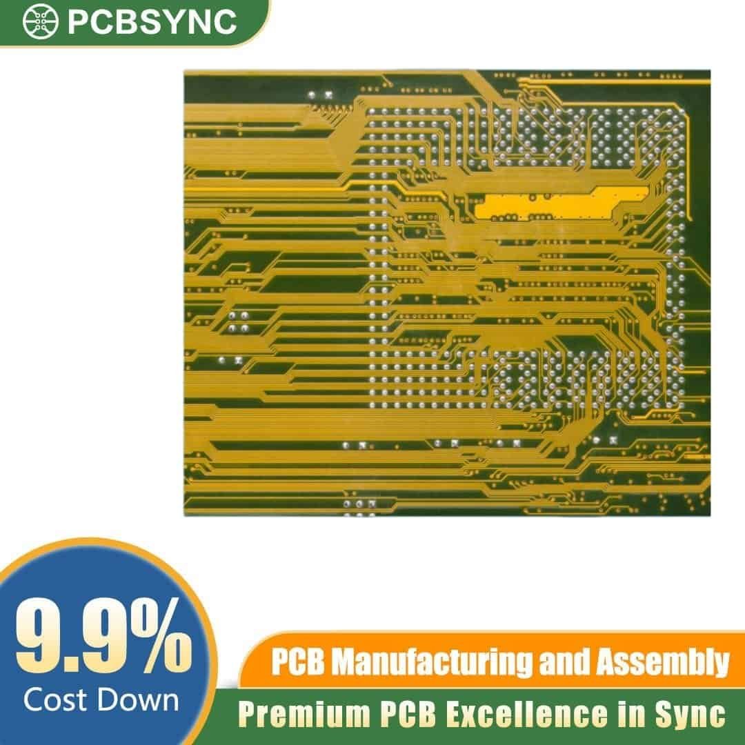
The 10-Layer 2+N+2 HDI PCB provides engineers and product developers with an advanced interconnect solution designed for strict high-speed build-up requirements. By integrating laser-drilled microvias across a symmetrical 2+N+2 architecture, this HDI PCB structure accommodates complex BGA routing and maximises board space efficiency for demanding, densely populated electronic devices.
Key Features of the 10-Layer 2+N+2 HDI PCB
-
Architectural Build-Up: 2+N+2 symmetrical layer structure engineered to support rigorous signal integrity requirements.
-
Advanced Routing: Incorporates staggered and stacked laser-drilled microvias, enabling the integration of ultra-fine pitch components.
-
Signal Performance: Strict impedance control parameters supporting high-speed data transmission and minimal signal loss.
-
Material Base: Manufactured utilising high-Tg FR4 and advanced dielectric materials to ensure structural and thermal stability under load.
-
Compliance: Fully compliant with IPC Class 2 and Class 3 fabrication standards.
Applications
This multi-layer interconnect technology is specified for industries requiring extreme component density and rapid data processing. Typical deployment includes 5G telecommunications infrastructure, aerospace flight control modules, advanced driver-assistance systems (ADAS), and robust industrial IoT gateways.
Why Choose PCBSYNC
PCBSYNC is a professional PCB fabrication, PCBA, and EMS manufacturer delivering precision-built electronics for aerospace, medical, automotive, industrial, and smart energy applications. We handle everything from rapid prototyping to mass production — including rigid, flexible, and rigid-flex PCBs, full turnkey assembly, component sourcing, AOI and X-ray inspection, and OEM/ODM support. Reliable boards. Consistent quality. From prototype to production — PCBSYNC.
Advance your product development with precision manufacturing. Request a quote today to discuss your technical specifications and production requirements with our engineering team.