Inquire: Call 0086-755-23203480, or reach out via the form below/your sales contact to discuss our design, manufacturing, and assembly capabilities.
Quote: Email your PCB files to Sales@pcbsync.com (Preferred for large files) or submit online. We will contact you promptly. Please ensure your email is correct.
Notes: For PCB fabrication, we require PCB design file in Gerber RS-274X format (most preferred), *.PCB/DDB (Protel, inform your program version) format or *.BRD (Eagle) format. For PCB assembly, we require PCB design file in above mentioned format, drilling file and BOM. Click to download BOM template To avoid file missing, please include all files into one folder and compress it into .zip or .rar format.
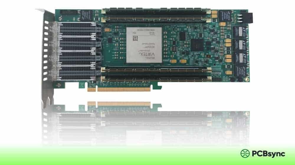
As a hardware engineer who’s spent over a decade working with programmable logic devices, I’ve seen Xilinx FPGA technology evolve from simple glue logic solutions to the powerhouse platforms driving everything from 5G base stations to autonomous vehicles. If you’re diving into the FPGA world—whether you’re designing your first development board or selecting silicon for a production project—this guide covers everything you need to know about Xilinx FPGA families and how to choose the right one for your application.
A Xilinx FPGA (Field-Programmable Gate Array) is a semiconductor device manufactured by Xilinx—now part of AMD since the $50 billion acquisition completed in February 2022. Unlike fixed-function chips like microcontrollers or ASICs, an FPGA contains an array of programmable logic blocks connected through configurable interconnects. This architecture allows engineers to implement custom digital circuits that can be reprogrammed after manufacturing.
Xilinx actually invented the first commercially viable FPGA back in 1985 with the XC2064, which featured 64 configurable logic blocks (CLBs). Since then, the company has dominated the FPGA market, holding approximately 51% market share globally. Their FPGAs range from entry-level devices with thousands of logic cells to massive chips containing over 6 million logic cells.
Xilinx FPGA Selection Tool
PCBSync Engineering Tools
Xilinx (AMD) FPGA Product Families
Spartan-7 Series
Cost-optimized FPGAs for high-volume, cost-sensitive applications. Ideal for I/O expansion, motor control, and sensor fusion.
6K-102K Logic CellsUp to 400 I/Os4.5Mb BRAM$10-$80 USD
Artix-7 Series
Lowest power 7 series FPGAs optimized for cost and power. Perfect for software-defined radio, machine vision, and industrial IoT.
12K-215K Logic CellsUp to 500 I/Os13Mb BRAM6.6Gb/s Transceivers$20-$150 USD
Artix UltraScale+
Next-gen cost-optimized FPGAs with enhanced DSP and connectivity. For edge computing and protocol bridging.
Up to 352K Logic Cells16.3Gb/s Transceivers24.2Mb BRAM$80-$300 USD
Kintex-7 Series
Best price-performance ratio. Optimized for wireless infrastructure, video broadcast, and data center applications.
65K-478K Logic CellsUp to 500 I/Os34Mb BRAM12.5Gb/s Transceivers$100-$800 USD
Kintex UltraScale+
High-performance with optimal price/performance/power. Ideal for 5G, machine learning, and video processing.
Up to 1.1M Logic Cells32.75Gb/s Transceivers76Mb BRAM2,880 DSP Slices$200-$2,000 USD
Virtex-7 Series
Highest performance and capacity FPGAs for demanding applications. ASIC replacement and high-bandwidth systems.
Up to 2M Logic Cells28.05Gb/s Transceivers68Mb BRAM3,600 DSP Slices$1,000-$10,000 USD
Virtex UltraScale+
Highest performance with 58G PAM4 transceivers. For 400G networking, aerospace, and high-end compute acceleration.
Up to 2.8M Logic Cells58Gb/s PAM4 Transceivers394Mb Memory12,288 DSP Slices$2,000-$30,000+ USD
Zynq-7000 SoC
All Programmable SoC with dual ARM Cortex-A9 cores + FPGA fabric. Perfect for embedded vision and motor control.
28K-444K Logic CellsDual ARM Cortex-A9Up to 1GHz CPU$30-$500 USD
Zynq UltraScale+ MPSoC
Multi-processor SoC with quad ARM Cortex-A53, dual Cortex-R5, Mali GPU + FPGA. For automotive ADAS and AI inference.
Up to 930K Logic CellsQuad ARM Cortex-A53Dual Cortex-R5Mali-400 GPU$100-$2,500 USD
Versal Adaptive SoC
Next-gen adaptive platform with AI Engines, ARM processors, and adaptable hardware. Industry’s first ACAP architecture.
AI Engines (400 TOPS)Dual ARM Cortex-A72112Gb/s TransceiversIntegrated NoC$500-$15,000+ USD
💡 Note on Pricing
Prices shown are estimated ranges for production quantities and may vary based on package, speed grade, and quantity. Contact distributors for accurate quotes.
FPGA Selection Wizard
Answer the questions below to get personalized FPGA recommendations for your design.
Compare FPGA Specifications
Application-Based FPGA Selection Guide
🏭
Industrial IoT
Spartan-7, Artix-7
📹
Video Processing
Kintex-7, Zynq-7000
📡
5G Wireless
Kintex US+, Zynq US+
🚗
Automotive ADAS
Zynq UltraScale+
🖥️
Data Center
Virtex US+, Alveo
✈️
Aerospace
Kintex US+, Virtex US+
🤖
AI/ML Inference
Versal AI, Zynq US+
🔬
Medical Imaging
Kintex-7, Zynq-7000
🎮
Consumer Electronics
Spartan-7, Artix-7
🔌
Motor Control
Spartan-7, Zynq-7000
📊
High-Freq Trading
Virtex US+, Alveo
🔒
Cryptography
Zynq US+, Versal
Application Details
FPGA Resource Estimator
Estimate FPGA resource requirements based on your design blocks.
PCBSync Engineering Tools | Xilinx and AMD are trademarks of AMD Inc.
Why Engineers Choose Xilinx FPGA Over Alternatives
From my experience on countless PCB projects, here’s why Xilinx remains the go-to choice:
Parallel Processing Power: Unlike sequential processors, FPGAs execute operations simultaneously, delivering massive throughput for signal processing and data-intensive applications
Reconfigurability: You can update the hardware logic in the field without respinning boards—a lifesaver when specifications change mid-project
Deterministic Timing: Critical for applications requiring precise timing like motor control, radar systems, and high-frequency trading
Lower NRE Costs: Compared to ASICs, you skip the expensive mask sets and lengthy fabrication cycles
Long Product Lifecycles: AMD guarantees 7 Series support through 2040 and UltraScale+ through 2045—excellent for aerospace and industrial applications
Understanding Xilinx FPGA Architecture
Before diving into specific families, let’s break down what’s inside every Xilinx FPGA. Understanding this architecture helps you make better resource allocation decisions during design.
Core Building Blocks
Component
Function
Design Consideration
CLBs (Configurable Logic Blocks)
Basic logic implementation using LUTs and flip-flops
More CLBs = more complex logic designs
Look-Up Tables (LUTs)
Implement combinational logic functions
6-input LUTs in modern devices
Flip-Flops (FFs)
Sequential logic and data storage
8 FFs per slice in 7 Series
Block RAM (BRAM)
High-speed on-chip memory
18Kb or 36Kb blocks, dual-port
DSP Slices
Dedicated multiply-accumulate blocks
Essential for signal processing
I/O Banks
Interface with external components
Different voltage standards per bank
Transceivers (GTx)
High-speed serial communication
Rates from 6.6 Gbps to 32.75 Gbps
Clock Management
PLLs and MMCMs for clock generation
Critical for timing closure
Process Technology Evolution
Xilinx FPGA process nodes have evolved significantly:
Now let’s get into the meat of this guide—the different Xilinx FPGA families and when to use each one.
Spartan Series: Entry-Level Excellence
The Spartan series sits at the foundation of the Xilinx FPGA lineup. I recommend these chips for cost-sensitive, high-volume applications where you need programmable logic but don’t require massive resources.
Spartan-7 Specifications
Parameter
Range
Logic Cells
6K – 102K
Block RAM
0.4 – 4.2 Mb
DSP Slices
10 – 160
Max I/O Pins
100 – 400
Max User I/O
250
Process
28nm
Best Applications for Spartan FPGAs
Industrial IoT sensor nodes
Consumer electronics
Low-cost motor drives
Basic video processing
Educational platforms
Simple protocol bridges
Pro Tip: If your design fits within Spartan resources, don’t over-engineer with a larger device. I’ve seen teams waste budget on Kintex parts when Spartan would have handled the job perfectly.
Artix Series: Transceiver-Optimized Performance
The Artix family delivers the sweet spot between cost and capability. What sets Artix apart from Spartan is the inclusion of high-speed transceivers and better DSP resources—making it ideal for applications requiring serial connectivity.
Artix-7 vs Artix UltraScale+ Comparison
Feature
Artix-7
Artix UltraScale+
Process Node
28nm
16nm
Max Logic Cells
215K
285K
Max Block RAM
13 Mb
22.5 Mb
Max DSP Slices
740
1,150
Transceiver Speed
6.6 Gbps
16.3 Gbps
Static Power
Baseline
50% lower
Artix Design Sweet Spots
Software-defined radio (SDR)
Multi-camera embedded vision
Portable medical devices
Battery-powered equipment
Point-to-point wireless links
Cost-optimized networking gear
The Artix-7 delivers 50% lower power and 35% lower cost compared to the older Spartan-6—making migration straightforward if you’re upgrading legacy designs.
Kintex Series: The Price-Performance King
In my opinion, Kintex represents the best value proposition in the Xilinx FPGA portfolio. You get serious computational muscle without the premium pricing of Virtex devices.
Kintex-7 Specifications
Parameter
Range
Logic Cells
66K – 478K
Block RAM
4.9 – 34 Mb
DSP Slices
240 – 1,920
Transceivers
Up to 32
Transceiver Speed
Up to 12.5 Gbps
PCIe Support
Gen2 x8
Kintex UltraScale/UltraScale+ Upgrades
Moving to Kintex UltraScale brings substantial improvements:
Feature
Kintex-7
Kintex UltraScale
Kintex UltraScale+
Max Logic Cells
478K
1.16M
1.15M
DSP Compute
740 GMAC/s
8.2 TeraMACs
9.8 TeraMACs
Transceiver Speed
12.5 Gbps
16.3 Gbps
32.75 Gbps
Memory Interface
DDR3
DDR4
DDR4 2666
PCIe
Gen2 x8
Gen3 x8
Gen3/4 x16
When to Choose Kintex
Data center accelerators
100G Ethernet networking
Advanced video processing (4K/8K)
Wireless infrastructure (5G fronthaul)
High-performance test equipment
Medical imaging systems
Virtex Series: Maximum Performance
Virtex is the flagship Xilinx FPGA family—designed for applications where performance trumps everything else. If you’re building cutting-edge telecommunications infrastructure, high-frequency trading systems, or defense platforms, Virtex is your tool.
Virtex-7 Capabilities
Parameter
Specification
Max Logic Cells
2,000,000
Max Block RAM
68 Mb
Max DSP Slices
3,600
Max Transceivers
96
Transceiver Speed
Up to 28.05 Gbps (GTZ)
3D IC Technology
Yes (Stacked Silicon Interconnect)
The Virtex-7 2000T was groundbreaking—it combined four FPGA dies on a silicon interposer to deliver 6.8 billion transistors in a single package. This stacked silicon interconnect (SSI) technology broke through monolithic silicon limitations.
Virtex UltraScale+ Performance
Feature
Virtex UltraScale+
Max Logic Cells
4.4M
Max Block RAM
600 Mb
Max UltraRAM
432 Mb
Max Transceivers
128
Transceiver Speed
32.75 Gbps
HBM2 Integration
Yes (up to 16 GB)
Virtex Application Areas
400G/800G networking line cards
Radar and electronic warfare systems
Particle physics experiments (CERN uses them)
Financial exchange infrastructure
Satellite communications
Machine learning inference acceleration
Cost Reality Check: Virtex devices command premium pricing. A Virtex UltraScale+ VU13P can cost several thousand dollars per unit. Make absolutely sure your requirements justify this investment before committing.
Zynq SoC: ARM + FPGA Integration
The Zynq family represents Xilinx’s most innovative product line—combining ARM Cortex processors with programmable logic on a single chip. This integration eliminates the traditional CPU+FPGA two-chip solution, reducing board complexity, power consumption, and system latency.
Zynq-7000 Architecture
Component
Specification
Processor
Dual-core ARM Cortex-A9 @ 1 GHz
FPGA Fabric
Artix-7 or Kintex-7 based
On-chip Memory
256 KB SRAM
External Memory
DDR3/DDR3L/DDR2 controller
Connectivity
USB, GigE, SPI, I2C, UART, CAN
AXI Interconnect
3,000+ PS-PL connections
The key advantage of Zynq is the processor-centric architecture. Unlike older FPGA+soft-processor combinations, Zynq boots immediately at power-up and runs standard operating systems (Linux, FreeRTOS) independently of the programmable logic.
Zynq UltraScale+ MPSoC
The next generation brings even more processing power:
Feature
Zynq UltraScale+ MPSoC
Application Processors
Quad-core ARM Cortex-A53 @ 1.5 GHz
Real-time Processors
Dual-core ARM Cortex-R5
GPU
ARM Mali-400 MP2
Video Codec
H.264/H.265 @ 4K60
FPGA Fabric
UltraScale+ architecture
Security
Secure boot, encryption, authentication
Zynq RFSoC: RF Direct Sampling
For wireless and radar applications, the Zynq RFSoC integrates high-speed ADCs (up to 4 GSPS) and DACs directly with the FPGA fabric—eliminating external RF data converters.
Zynq RFSoC Feature
Specification
ADC Channels
Up to 16
ADC Sample Rate
2-5 GSPS
DAC Channels
Up to 16
DAC Sample Rate
6.5+ GSPS
Digital Down/Up Conversion
Hardened blocks
Best Zynq Applications
Advanced driver assistance systems (ADAS)
Industrial automation and robotics
5G small cells and massive MIMO
Software-defined radio platforms
Embedded vision systems
Motor control with real-time processing
Xilinx FPGA Selection Guide: How to Choose
After working through hundreds of FPGA selection decisions, here’s my systematic approach:
Step 1: Define Your Resource Requirements
Calculate your needs:
Resource
How to Estimate
Logic Cells
RTL synthesis report + 30% margin
Block RAM
Data buffers, FIFOs, lookup tables
DSP Slices
Filters, FFTs, MACs needed
Transceivers
Serial interfaces count and speed
I/O
Pin count by voltage standard
Step 2: Match to Family
If You Need…
Consider…
Lowest cost, simple logic
Spartan-7
Cost-optimized with transceivers
Artix-7/UltraScale+
Best price-performance ratio
Kintex-7/UltraScale+
Maximum performance, no compromises
Virtex UltraScale+
Embedded processing + FPGA
Zynq-7000 or UltraScale+
RF direct sampling
Zynq RFSoC
Step 3: Consider These Factors
Power Budget: UltraScale+ devices deliver 2x performance per watt versus 7 Series
Temperature Range: Industrial grade (-40°C to 100°C) adds cost
Longevity: 7 Series support extends to 2040
Tool Support: Vivado supports 7 Series and newer; ISE required for older devices
Development Board Availability: Prototype before committing
Xilinx FPGA Development Tools and Software
Vivado Design Suite
Vivado is the primary development environment for Xilinx FPGA designs targeting 7 Series and newer devices. It replaced the older ISE Design Suite and represents a complete architectural rewrite.
Vivado Edition
Supported Devices
Cost
Standard (WebPACK)
Limited subset
Free
Enterprise
All devices
$4,395+
Vivado includes:
HDL synthesis and implementation
Built-in simulator
IP Integrator for block-based design
High-Level Synthesis (HLS) for C/C++ to RTL conversion
ChipScope debugging
Power analysis tools
Vitis Unified Software Platform
For Zynq and Versal designs, Vitis provides the software development environment:
Embedded software IDE (Eclipse-based)
PetaLinux for embedded Linux builds
AI engine programming
Acceleration library support
Getting Started: Essential Resources
Here are the resources I recommend for anyone starting with Xilinx FPGAs:
Official AMD/Xilinx Resources
Resource
URL
Purpose
Vivado Download
xilinx.com/support/download.html
Design tools
Documentation Portal
docs.xilinx.com
Technical docs
Product Selection Guide
7 Series Product Selection Guide PDF
Device comparison
University Program
xilinx.com/support/university.html
Academic resources
GitHub Repositories
github.com/Xilinx
Reference designs
Recommended Development Boards
Board
Family
Price Range
Best For
Basys 3
Artix-7
~$150
Learning/education
Nexys A7
Artix-7
~$270
Academic projects
ZedBoard
Zynq-7000
~$500
Embedded Linux
ZCU104
Zynq UltraScale+
~$1,200
AI/ML development
KCU105
Kintex UltraScale
~$2,500
High-speed connectivity
Alveo U250
Virtex UltraScale+
~$6,000
Data center acceleration
Learning Path
Master an HDL: Start with Verilog or VHDL—SystemVerilog for modern designs
Complete Vivado Tutorials: Work through the official design flow tutorials
Study Reference Designs: Xilinx provides excellent example code
Join the Community: Xilinx Forums, Reddit r/FPGA, EEVblog forums
Real-World Xilinx FPGA Applications
Let me share some practical examples from my experience and industry case studies:
Telecommunications and 5G
Samsung uses Versal adaptive SoCs to build flexible 5G base station platforms that can adapt to evolving standards. The reconfigurability means operators don’t need hardware replacements when 3GPP releases specification updates.
Automotive ADAS
Subaru selected Zynq UltraScale+ MPSoC for their next-generation advanced driver assistance systems. The combination of real-time ARM cores and FPGA fabric handles sensor fusion, object detection, and decision-making with deterministic timing.
Data Center Acceleration
Microsoft deploys FPGAs in Azure data centers for Bing search acceleration and AI inference. The parallel processing capability delivers better performance-per-watt than GPUs for specific workloads like network packet processing.
Medical Imaging
Xilinx FPGAs power CT scanners, MRI systems, and ultrasound equipment where real-time image reconstruction requires massive computational throughput with strict latency constraints.
Financial Trading
High-frequency trading firms use Virtex FPGAs to achieve sub-microsecond trade execution. The deterministic timing eliminates jitter that software-based systems cannot avoid.
Common Xilinx FPGA Design Challenges and Solutions
Challenge 1: Timing Closure
Problem: Design doesn’t meet frequency targets.
Solutions:
Use Vivado’s Report QoR Suggestions
Add pipeline registers in critical paths
Constrain clocks properly in XDC files
Consider incremental compile for small changes
Challenge 2: Resource Utilization
Problem: Design doesn’t fit in chosen device.
Solutions:
Review synthesis reports for resource hogs
Use DSP slices instead of fabric multipliers
Implement memories using Block RAM, not LUTs
Consider resource sharing for infrequent operations
Challenge 3: Power Consumption
Problem: Device exceeds thermal budget.
Solutions:
Use clock gating for inactive modules
Select lower speed grade if timing allows
Enable Vivado’s power optimization
Consider UltraScale+ for better efficiency
Challenge 4: Signal Integrity
Problem: High-speed interfaces failing.
Solutions:
Follow Xilinx PCB guidelines strictly
Use proper termination schemes
Ensure adequate power plane design
Implement IBERT testing for transceivers
Future of Xilinx FPGA Under AMD
The AMD acquisition positions Xilinx technology for deeper integration with AMD CPUs and GPUs. Key developments to watch:
Versal ACAP: Adaptive Compute Acceleration Platform combining scalar processors, adaptable engines, and AI engines
Chiplet Integration: Potential FPGA fabric integration with AMD Ryzen/EPYC processors
Software Convergence: Unified programming models across AMD hardware
AI Focus: Enhanced machine learning acceleration capabilities
AMD has committed to maintaining the Xilinx product lines and extending support for existing devices through 2040-2045.
Frequently Asked Questions (FAQs)
Is Xilinx still a separate company?
No. AMD completed its acquisition of Xilinx in February 2022 for approximately $50 billion. The Xilinx brand was phased out in June 2023, and products are now marketed under AMD. However, the product lines (Spartan, Artix, Kintex, Virtex, Zynq) continue with the same architectures.
Which Xilinx FPGA is best for beginners?
I recommend starting with an Artix-7 or Spartan-7 based development board like the Basys 3 or Nexys A7 from Digilent. These devices offer enough resources for meaningful projects while being supported by the free Vivado WebPACK edition. For embedded systems work, the PYNQ-Z2 board provides an excellent introduction to Zynq SoCs with Python-based development.
What programming language is used for Xilinx FPGAs?
Xilinx FPGAs are primarily programmed using Hardware Description Languages (HDLs)—specifically Verilog, VHDL, or SystemVerilog. For higher-level development, Vivado HLS accepts C/C++ code and generates RTL automatically. Zynq devices additionally support standard software languages like C, C++, and Python for the ARM processor side.
How much does a Xilinx FPGA cost?
Pricing varies dramatically by family and device:
Family
Typical Unit Price (Low Volume)
Spartan-7
$10 – $100
Artix-7
$30 – $300
Kintex-7
$200 – $2,000
Virtex-7
$1,000 – $10,000+
Zynq-7000
$50 – $500
UltraScale+
$500 – $30,000+
Development boards range from $150 for entry-level to $10,000+ for high-end evaluation kits.
Can Xilinx FPGAs be used for AI and machine learning?
Absolutely. Xilinx FPGAs excel at AI inference workloads due to their parallel processing architecture and flexible datapath widths. The Versal AI Core and AI Edge series include dedicated AI engines optimized for neural network acceleration. AMD acquired DeepPhi Technology in 2018 specifically to enhance AI capabilities. Major cloud providers including AWS, Azure, and Alibaba offer FPGA instances for AI acceleration.
Xilinx FPGA vs Competitors: How Does It Stack Up?
Understanding how Xilinx compares to other FPGA vendors helps you make informed procurement decisions.
Xilinx vs Intel (Altera)
Intel acquired Altera in 2015 for $16.7 billion, creating the second-largest FPGA vendor. Here’s how they compare:
Aspect
Xilinx (AMD)
Intel (Altera)
Market Share
~51%
~34%
Primary Tool
Vivado
Quartus Prime
High-End Family
Virtex UltraScale+
Agilex
Mid-Range Family
Kintex
Stratix
Entry-Level
Spartan/Artix
Cyclone/MAX
SoC Integration
Zynq (ARM)
Stratix 10 SX (ARM)
Process Leadership
16nm FinFET
10nm Intel
HLS Support
Vitis HLS
Intel HLS Compiler
My Take: Xilinx has traditionally led in software tools and documentation quality. Intel’s integration with their fab capabilities offers some unique advantages at advanced nodes. For most applications, both vendors offer comparable solutions—your choice often depends on existing toolchain investments and design team expertise.
Xilinx vs Lattice Semiconductor
Lattice specializes in low-power, small-footprint FPGAs:
Aspect
Xilinx
Lattice
Strength
Performance, capacity
Ultra-low power
Typical Power
mW to tens of Watts
µW to low mW
Largest Device
Millions of LUTs
~100K LUTs
Best For
High performance
Battery-powered, edge
Tool Cost
Free WebPACK available
Free tools available
When to Choose Lattice: If your application prioritizes battery life over raw performance—think wearables, IoT sensors, or always-on edge devices.
Xilinx vs Microchip (Microsemi)
Microchip acquired Microsemi (previously Actel) and focuses on specialized markets:
Aspect
Xilinx
Microchip
Strength
General purpose
Radiation-hardened, secure
Key Markets
Consumer to defense
Aerospace, defense, nuclear
Flash-Based
No (SRAM-based)
Yes (non-volatile)
Instant-On
No (requires config)
Yes
Space-Grade
XQR devices
RT ProASIC3, RTAX
When to Choose Microchip: Mission-critical applications requiring non-volatile configuration, single-event upset immunity, or security-focused designs.
Deep Dive: Xilinx 7 Series FPGA Family
The 7 Series remains the workhorse of Xilinx’s portfolio, still widely deployed in new designs due to its maturity, excellent documentation, and long-term support commitment.
Unified 28nm Architecture Benefits
All 7 Series devices share a common architecture, meaning:
IP cores work across all families without modification
Design migration between families requires minimal changes
Engineers can start on Artix-7 and scale to Virtex-7 if needed
Consistent Vivado workflow regardless of target device
Routing Architecture: UltraScale introduces a redesigned routing fabric with:
75% more routing resources per logic cell
Better signal integrity at higher frequencies
Reduced congestion for dense designs
More efficient wire utilization
Enhanced DSP Blocks: The DSP48E2 slice in UltraScale offers:
27×18 multiplier (vs 25×18 in 7 Series)
Improved pre-adder functionality
Better cascading for large filter implementations
Floating-point support with IP cores
UltraRAM: UltraScale+ introduced a new memory primitive:
Feature
Block RAM
UltraRAM
Size
36 Kb
288 Kb
Ports
Dual-port
Dual-port
Cascade
Yes
Native chaining
Best For
FIFOs, buffers
Large data structures
UltraScale Device Comparison
Device
Logic Cells
Block RAM
DSP Slices
Transceivers
KU035
443K
27 Mb
1,700
16
KU115
1,160K
76 Mb
5,520
64
VU095
1,099K
68 Mb
768
64
VU190
2,191K
133 Mb
1,800
96
PCB Design Considerations for Xilinx FPGAs
As someone who’s laid out dozens of FPGA boards, here are critical considerations that determine success or failure.
Power Distribution Network (PDN) Design
FPGAs have multiple power rails requiring careful attention:
Rail
Typical Voltage
Purpose
Decoupling Strategy
VCCINT
0.85V – 1.0V
Core logic
High-density MLCCs, bulk caps
VCCAUX
1.8V
Auxiliary circuits
Mixed MLCC values
VCCBRAM
1.0V
Block RAM
Dedicated bypass caps
VCCO
1.2V – 3.3V
I/O banks
Per-bank decoupling
VCCMGT
Varies
Transceivers
Ultra-low ESL caps
Power Sequencing: Most Xilinx FPGAs require specific power-up sequences. VCCINT typically must ramp before VCCO to prevent latch-up. Use dedicated sequencing ICs or design your power supply with appropriate enable delays.
High-Speed Signal Integrity
For multi-gigabit transceivers:
Parameter
Recommendation
Trace Impedance
50Ω single-ended, 100Ω differential
Length Matching
<5 mil within differential pair
Via Count
Minimize—each via adds discontinuity
Reference Plane
Continuous ground, no splits
Coupling Capacitors
100nF for AC coupling
Crosstalk Mitigation:
Maintain 3x trace width spacing between differential pairs
Use ground guard traces for sensitive signals
Separate high-speed and low-speed routing regions
Consider stripline for inner layers
Configuration and Boot Design
Configuration Mode
Pins Required
Best For
Master Serial
3
Production, secure
Master SPI
4-8 (quad)
Fast configuration
Slave Serial
3
JTAG chain
Master BPI
26+
Fast, parallel boot
JTAG Only
4
Development, debug
Configuration Storage Options:
Serial NOR Flash (most common)—SPI interface, various densities
Parallel NOR Flash—faster load times, more pins
CPLD—secure boot, design protection
Processor—dynamic reconfiguration scenarios
Thermal Management
FPGA power dissipation requires active thermal design:
Package Style
Typical θJA
Cooling Requirement
QFN/BGA Small
15-25°C/W
PCB heatsinking
BGA Medium
8-15°C/W
Heatsink required
BGA Large
4-8°C/W
Active cooling
Flip-chip BGA
0.5-2°C/W
Advanced cooling
Use Xilinx Power Estimator (XPE) early in design to estimate power and plan thermal solutions before board layout begins.
ILA allows capturing internal signals during hardware operation:
Feature
Capability
Probe Width
Up to 4,096 bits
Sample Depth
1K to 128K samples
Trigger
Boolean expressions
Storage
BRAM or URAM
ILA Best Practices:
Mark debug nets with (* mark_debug = “true” *) attribute
Use ILA Dashboard in Hardware Manager
Keep debug cores minimal in production builds
Pipeline signals to debug probes to avoid timing impact
Virtual I/O (VIO)
VIO provides runtime control of design parameters:
Use Case
VIO Configuration
Register writes
Output probes to target
Status monitoring
Input probes from signals
Mode selection
Output probes to muxes
Threshold adjustment
Output probes to comparators
System ILA for AXI Debugging
For Zynq and MicroBlaze designs, System ILA captures AXI transactions:
AXI Channel
Signals Captured
Write Address
AWADDR, AWLEN, AWSIZE
Write Data
WDATA, WSTRB, WLAST
Write Response
BRESP, BVALID
Read Address
ARADDR, ARLEN, ARSIZE
Read Data
RDATA, RRESP, RLAST
Industry-Specific Xilinx FPGA Applications
Aerospace and Defense Applications
Xilinx offers specialized grades for harsh environments:
Grade
Temperature Range
Key Feature
Commercial
0°C to +85°C
Standard
Industrial
-40°C to +100°C
Extended temp
Automotive (XA)
-40°C to +125°C
AEC-Q100 qualified
Defense (XQ)
-55°C to +125°C
MIL-STD screening
Space (XQR)
Radiation tolerant
SEU hardening
Aerospace Use Cases:
Satellite payload processing
Radar signal processing
Electronic warfare systems
Flight control systems
Secure communications
Automotive Applications
Zynq UltraScale+ XA devices power modern vehicles:
Application
Xilinx Solution
ADAS Camera Processing
Zynq UltraScale+ EV
LiDAR Data Processing
Kintex UltraScale
Central Gateway
Zynq-7000 XA
Infotainment
Zynq UltraScale+ CG
V2X Communications
Zynq RFSoC
Medical Device Applications
FPGAs enable real-time medical imaging:
Application
Requirements Met
Ultrasound
Beamforming, real-time imaging
CT Scanner
Reconstruction algorithms
MRI
Gradient coil control, imaging
Patient Monitoring
Multi-channel signal processing
Surgical Robots
Deterministic control loops
Conclusion
Xilinx FPGA technology—now under the AMD umbrella—remains the industry standard for programmable logic. Whether you’re designing a simple protocol bridge with Spartan-7 or building 400G networking infrastructure with Virtex UltraScale+, understanding the product families and their capabilities is essential for making the right selection.
The key takeaway: match your requirements to the appropriate family. Don’t overspend on Virtex when Kintex delivers what you need, but don’t underspec and paint yourself into a corner either. Leave margin for design growth, and always prototype on a development board before committing to production silicon.
The unified architecture across 7 Series and UltraScale families means skills and IP transfer readily between devices. Start with a development board, work through the Vivado tutorials, and build increasingly complex designs. The investment in learning FPGA design pays dividends across your engineering career.
For those just starting out, the combination of accessible development boards, free Vivado WebPACK, and extensive online resources makes this an excellent time to learn FPGA design. The skills transfer directly to real-world engineering projects, and the demand for FPGA expertise continues growing across industries from automotive to aerospace to artificial intelligence.
Inquire: Call 0086-755-23203480, or reach out via the form below/your sales contact to discuss our design, manufacturing, and assembly capabilities.
Quote: Email your PCB files to Sales@pcbsync.com (Preferred for large files) or submit online. We will contact you promptly. Please ensure your email is correct.
Notes: For PCB fabrication, we require PCB design file in Gerber RS-274X format (most preferred), *.PCB/DDB (Protel, inform your program version) format or *.BRD (Eagle) format. For PCB assembly, we require PCB design file in above mentioned format, drilling file and BOM. Click to download BOM template To avoid file missing, please include all files into one folder and compress it into .zip or .rar format.


