Inquire: Call 0086-755-23203480, or reach out via the form below/your sales contact to discuss our design, manufacturing, and assembly capabilities.
Quote: Email your PCB files to Sales@pcbsync.com (Preferred for large files) or submit online. We will contact you promptly. Please ensure your email is correct.
Notes: For PCB fabrication, we require PCB design file in Gerber RS-274X format (most preferred), *.PCB/DDB (Protel, inform your program version) format or *.BRD (Eagle) format. For PCB assembly, we require PCB design file in above mentioned format, drilling file and BOM. Click to download BOM template To avoid file missing, please include all files into one folder and compress it into .zip or .rar format.
If you’ve ever spent hours troubleshooting a failed PCB only to discover a hidden solder void under a BGA, you know exactly why X-Ray inspection matters. I’ve been there—staring at a board that passed every optical test but still wouldn’t function. That’s when you realize that what you can’t see can absolutely hurt you.
X-Ray inspection has become the backbone of quality control in modern electronics manufacturing. As our boards get denser, components shrink, and packages like BGAs, QFNs, and CSPs hide their solder joints underneath, traditional visual methods simply don’t cut it anymore. This guide covers everything you need to know about implementing X-Ray inspection in your PCB manufacturing and assembly process—from the physics behind it to practical defect detection strategies.
X-Ray inspection, often called Automated X-Ray Inspection (AXI), is a non-destructive testing method that uses X-ray radiation to examine the internal structures of printed circuit boards and their assemblies. Unlike your eyes or a camera, X-rays penetrate through materials, allowing you to see what’s happening inside solder joints, under component packages, and within multilayer boards.
The technology works on a simple principle: different materials absorb X-rays at different rates based on their atomic weight and density. Heavy elements like lead and tin (found in solder) absorb more X-rays and appear darker in the resulting image. Lighter materials like silicon, plastic, and the FR-4 substrate let more X-rays pass through and appear lighter or transparent.
Why X-Ray Inspection Has Become Essential
Ten years ago, you could get away with visual inspection and maybe some AOI for most boards. That’s no longer the case. Here’s why X-Ray inspection has moved from “nice to have” to “absolutely necessary”:
BGA packages now dominate high-performance designs. When you have 500+ solder balls hidden under a processor package, there’s literally no other way to verify those connections.
QFN and LGA packages have exploded in popularity. These leadless packages place all their connections underneath the component body—invisible to optical systems.
Board density keeps increasing. With 0201 and even 01005 components becoming common, the tolerance for defects has shrunk dramatically.
Industry standards demand it. IPC-A-610 Class 3 requirements for aerospace and medical devices essentially mandate X-Ray inspection for array packages.
How X-Ray Inspection Works: The Technical Breakdown
Understanding how your X-Ray system works helps you get better results from it. Here’s what’s actually happening inside that machine.
Core Components of an X-Ray System
Every X-Ray inspection system consists of three fundamental components working together:
Component
Function
Key Specifications
X-Ray Tube
Generates X-ray photons by accelerating electrons into a metal target
Voltage (kV), power (W), spot size (μm)
Sample Platform
Holds and manipulates the PCB for different viewing angles
XYZ movement, tilt capability, rotation
Detector
Captures transmitted X-rays and converts them to digital images
Resolution, sensitivity, frame rate
The X-ray tube is where everything starts. Electrons are accelerated at high voltage and slammed into a metal target (usually tungsten). This collision produces X-ray photons. The spot size—how small that impact point is—directly affects your image resolution. For BGA inspection, you generally need a spot size of 5μm or smaller. For advanced packaging like flip-chip, you might need sub-micron resolution.
The Image Formation Process
When X-rays pass through your PCB assembly, different materials attenuate them differently:
Solder joints (high density) absorb most X-rays → appear dark in the image
Copper traces (medium density) absorb some X-rays → appear gray
FR-4 substrate (low density) absorbs few X-rays → appears light
Air voids (no density) absorb nothing → appear very light/white
This grayscale contrast is what allows you to identify defects. A good solder ball looks uniformly dark and round. A void shows up as a light spot within that dark circle. A bridge appears as dark solder connecting two balls that should be separate.
2D vs. 2.5D vs. 3D X-Ray Inspection
Not all X-Ray systems are created equal. The imaging mode you choose significantly impacts what defects you can detect.
Imaging Mode
How It Works
Best For
Limitations
2D X-Ray
Single top-down view through the entire board
Quick screening, single-sided boards
Overlapping features from double-sided assemblies
2.5D X-Ray (Oblique)
Angled views that separate overlapping layers
THT inspection, BGA ball shape analysis
Limited layer separation
3D CT X-Ray
Multiple projections reconstructed into volumetric data
Complete internal analysis, void location
Slower, more expensive
For most production environments, 2.5D systems offer the best balance of speed and capability. True 3D CT is typically reserved for failure analysis or high-reliability applications where you need to know exactly where a void sits within a solder ball.
Types of Defects Detected by X-Ray Inspection
Here’s where X-Ray inspection really earns its keep. These are the defects that optical inspection simply cannot catch.
Solder Voids and Void Percentage Analysis
Voids are trapped gas pockets within solder joints—and they’re more common than you might think. Small voids (under 10% of joint area) usually aren’t a reliability concern. But as void percentage increases, so do the risks:
Reduced thermal conductivity — Critical for power devices that need to dissipate heat
Weakened mechanical strength — The joint is more likely to crack under thermal cycling
Increased electrical resistance — Can cause voltage drops in high-current applications
IPC-7095 provides detailed guidance on acceptable void levels. For Class 2 products (general electronics), the typical limit is 25% total void area. Class 3 products (high reliability) often require less than 10% voiding, particularly at the interconnection interfaces.
Pro tip: When analyzing voids, location matters as much as size. A 15% void in the center of a BGA ball is less concerning than a 10% void at the pad interface. Modern X-Ray systems with laminography can tell you exactly where that void sits.
Void Types and Classification
IPC-7095 identifies five distinct types of voids that can occur in BGA solder joints:
Void Type
Location
Typical Cause
Reliability Impact
Type A
Within solder ball body
Paste outgassing
Low if <25%
Type B
At ball-to-pad interface
Poor wetting, oxidation
High—weakens connection
Type C
At ball-to-component interface
Component finish issues
High—affects reliability
Type D
Planar void (large, flat)
Severe outgassing
Moderate to high
Type E
Micro-voiding (many small voids)
Paste chemistry issues
Cumulative effect
Understanding which type of void you’re seeing helps identify the root cause and implement effective corrective action.
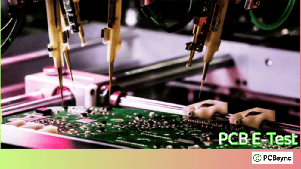
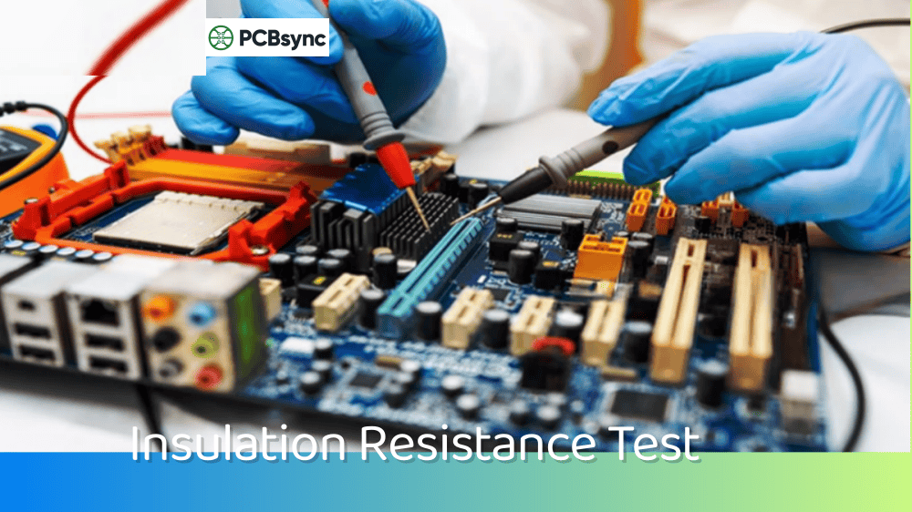
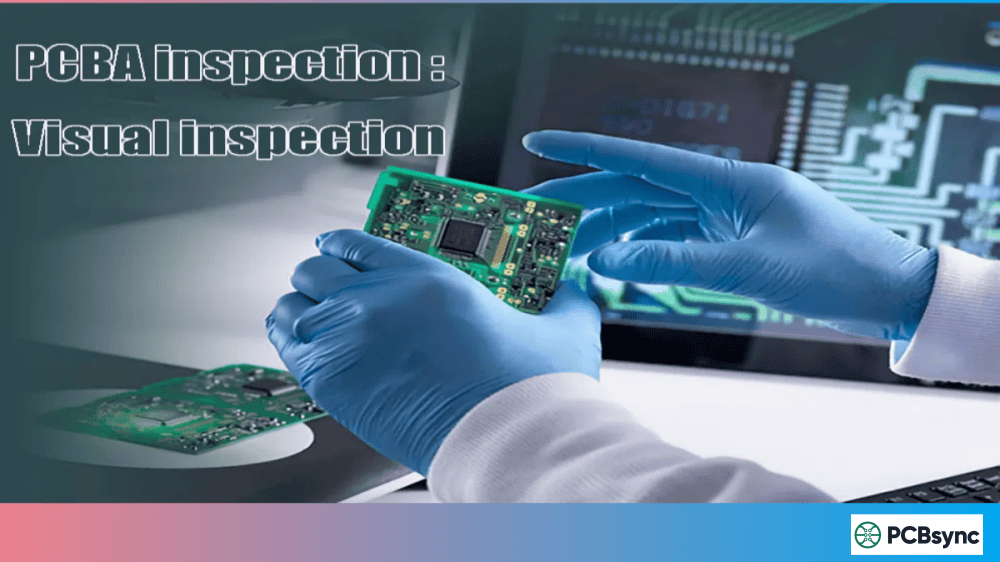
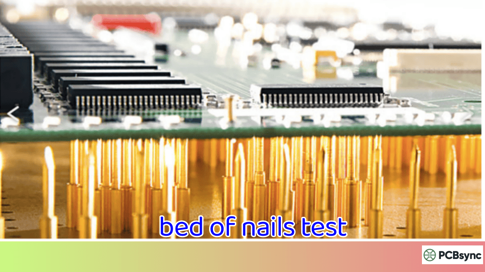
Read more about PCBSync electronic testing method:
Ball Grid Array inspection is probably the single most important application of X-Ray in PCB assembly. Here’s what you’re looking for:
Defect Type
X-Ray Appearance
Root Cause
Impact
Solder bridges/shorts
Dark connection between adjacent balls
Excess solder, misalignment
Short circuit
Open connections
Light gap between ball and pad
Insufficient solder, warpage
No electrical connection
Head-in-pillow (HIP)
Ball appears separated with irregular interface
Component warpage during reflow
Intermittent connection
Missing balls
Absent dark circle in the array pattern
Manufacturing defect, handling damage
Open circuit
Voiding
Light spots within dark solder balls
Outgassing, moisture, paste issues
Reduced reliability
Ball size variation
Inconsistent ball diameters
Paste volume issues
Uneven standoff height
Head-in-pillow defects deserve special attention because they’re particularly tricky. The solder ball and paste both melt during reflow, but component warpage prevents them from coalescing. You end up with what looks like a connection but is actually two separate surfaces barely touching. These cause the worst kind of failures—intermittent ones that pass functional test but fail in the field.
QFN and Bottom Termination Component (BTC) Inspection
QFN packages present unique inspection challenges because of their large central thermal pad. Current draft IPC guidance suggests accepting up to 50% voiding under the central pad for most applications, though this varies based on thermal requirements.
Edge terminations on QFNs are more critical—these carry the electrical signals. X-Ray can verify that solder has properly wetted to these small pads, which is impossible to confirm optically.
Through-Hole Solder Fill Verification
For mixed-technology boards with through-hole components, X-Ray inspection verifies proper barrel fill. You can see whether solder has wicked up through the via and formed adequate fillets on both sides. This is particularly important for:
Connectors subjected to mechanical stress
Power delivery components carrying high current
Military and aerospace applications requiring 75%+ barrel fill
Internal Layer Defects in Multilayer PCBs
Beyond assembly inspection, X-Ray can reveal defects within the bare board itself:
Via barrel cracks
Delamination between layers
Drill registration errors
Internal shorts from copper migration
These defects often cause field failures that are extremely difficult to diagnose without X-Ray capability.
X-Ray Inspection vs. AOI: Understanding When to Use Each
One question I hear constantly: “Can’t AOI do everything X-Ray does?” The short answer is no. They’re complementary technologies, not competitors.
Comparison of Detection Capabilities
Defect Category
AOI
X-Ray
Notes
Surface solder bridges
✅ Yes
✅ Yes
AOI is faster for visible bridges
BGA solder bridges
❌ No
✅ Yes
Hidden under package
Missing components
✅ Yes
✅ Yes
AOI preferred for speed
Component polarity
✅ Yes
⚠️ Limited
AOI reads markings
Tombstoning
✅ Yes
✅ Yes
Both effective
Solder voids
❌ No
✅ Yes
Voids are internal
BGA ball integrity
❌ No
✅ Yes
Hidden connections
QFN terminations
❌ No
✅ Yes
Under component body
Through-hole fill
⚠️ Partial
✅ Yes
X-Ray sees internal fill
Head-in-pillow
❌ No
✅ Yes
Requires X-Ray analysis
Practical Inspection Strategy
For a typical SMT line, here’s what works well:
Post-placement AOI — Catch placement errors before reflow while rework is easy
Post-reflow AOI — Inspect all visible solder joints
Post-reflow X-Ray — Inspect BGAs, QFNs, and other hidden-joint packages
This combination catches over 95% of defects. The X-Ray step adds cycle time but is non-negotiable for boards with array packages.
Industry Applications of X-Ray Inspection
X-Ray inspection requirements vary significantly by industry. Here’s what drives adoption in different sectors.
Aerospace and Defense
Zero-defect requirements make X-Ray inspection mandatory for virtually all assemblies. Every BGA, every hidden joint must be verified. IPC Class 3 specifications apply across the board, with void limits often stricter than standard guidelines.
Typical requirements:
100% X-Ray inspection of all area array packages
Void percentage documentation for every joint
Image archival for traceability (often 10+ years)
Medical Devices
Life-critical equipment demands the same rigor as aerospace. FDA regulations and ISO 13485 quality systems require documented evidence of solder joint quality. X-Ray images become part of the Device History Record.
Automotive Electronics
As vehicles incorporate more electronics—especially for ADAS and EV powertrains—reliability requirements have tightened dramatically. AEC-Q standards and OEM-specific requirements increasingly mandate X-Ray inspection for:
Engine control units (ECUs)
Battery management systems
Power electronics
Safety-critical sensors
Consumer Electronics
High-volume consumer products typically use statistical sampling rather than 100% inspection. X-Ray systems with fast throughput (under 30 seconds per board) enable inspection of representative samples from each lot.
Telecommunications and 5G Infrastructure
High-frequency boards for 5G require excellent solder joint quality to maintain signal integrity. X-Ray inspection helps identify voids and irregularities that could affect RF performance.
Key inspection points for telecom applications include:
RF shielding can attachments and solder joints
High-density array packages for baseband processors
Power amplifier thermal interfaces
Antenna feed connections
The push toward higher frequencies makes solder joint quality even more critical, as signal degradation from poor connections becomes more pronounced at millimeter-wave frequencies.
Industrial and IoT Applications
Industrial electronics operating in harsh environments—extreme temperatures, vibration, moisture—require robust solder joints. X-Ray inspection verifies that connections will survive these conditions. IoT devices, while often cost-sensitive, increasingly incorporate X-Ray inspection for:
Sensor module connections
Wireless communication modules
Power management circuits
Battery management systems
Benefits of Implementing X-Ray Inspection
The ROI on X-Ray inspection equipment comes from several sources:
Early Defect Detection
Finding a BGA defect before the board ships costs a fraction of finding it after the product is in customers’ hands. Field failure costs can run 10-100x higher than in-process detection when you factor in:
Shipping and handling
Technician time for diagnosis
Replacement parts
Customer relationship damage
Potential warranty claims
Process Optimization
X-Ray doesn’t just find defects—it helps you understand why they’re happening. Seeing consistent voiding patterns tells you something about your reflow profile. Noticing repeated head-in-pillow defects points to component warpage issues. This feedback loop drives continuous improvement.
Specific process adjustments that X-Ray data can inform include:
Reflow profile tuning — Void patterns indicate whether you need longer soak times, different peak temperatures, or adjusted cooling rates
Solder paste selection — Persistent voiding may point to paste chemistry issues that require a different formulation
Stencil design optimization — Insufficient solder or excessive voiding can indicate aperture size problems
Component placement accuracy — Misalignment visible in X-Ray images may require machine calibration
Storage and handling — Moisture-related defects like popcorning reveal handling procedure issues
Compliance with Industry Standards
Meeting IPC-A-610 Class 3 requirements, customer specifications, or industry regulations often isn’t optional. X-Ray inspection provides documented evidence of compliance that auditors and customers require.
Reduced Scrap and Rework Costs
Catching defects at the inspection station—while the board is still on the line and the oven is still warm—means lower rework costs. Identifying systematic problems early prevents entire batches from being built with the same defect.
Limitations and Considerations
X-Ray inspection isn’t perfect. Understanding its limitations helps you use it effectively.
What X-Ray Cannot Detect
Limitation
Why It Matters
Alternative Approach
Component value errors
X-Ray sees structure, not electrical properties
Flying probe, ICT
Wrong component (same package)
Can’t distinguish between similar-looking parts
AOI with OCR, ICT
Functional defects
No electrical testing capability
Functional test
Surface contamination
X-Ray penetrates through residues
AOI, visual inspection
Incorrect polarity (some cases)
May not see marking orientation
AOI inspection
Speed vs. Resolution Trade-offs
High-resolution inspection takes time. A detailed 3D CT scan might take several minutes per component—acceptable for failure analysis but not for production. You need to balance:
Resolution requirements based on the smallest feature you need to see
Throughput requirements based on line takt time
Sampling strategy to balance coverage with speed
Cost Considerations
X-Ray equipment represents a significant capital investment:
Entry-level 2D systems: $50,000 – $150,000
Production 2.5D systems: $150,000 – $400,000
3D CT systems: $400,000 – $1,000,000+
The ROI calculation should consider not just defect detection but also the cost of undetected failures, customer requirements, and competitive positioning.
Radiation Safety
Modern X-Ray inspection systems are fully shielded and meet all regulatory requirements for radiation safety. Surface leakage on quality systems is typically less than 1 μSv/hour—well below any safety threshold. Still, proper training and compliance with local regulations are essential.
Operator Training Requirements
Getting accurate results from X-Ray inspection requires trained operators who understand both the equipment and the defects they’re looking for. Key training areas include:
Image interpretation — Understanding what good and bad solder joints look like in X-Ray images
System operation — Proper setup, calibration, and maintenance procedures
Defect classification — Knowing which defects are acceptable vs. rejectable per applicable standards
Documentation — Properly recording and archiving inspection results
Most equipment manufacturers offer certification programs, and IPC provides industry-recognized training for inspection personnel.
Integration Challenges
Bringing X-Ray inspection into an existing production line requires careful planning:
Floor space — X-Ray systems require dedicated space with proper shielding
Cycle time impact — Adding inspection time affects overall throughput
Data management — Image storage and retrieval needs must be addressed
Workflow integration — Systems should communicate with MES for traceability
Future Trends in X-Ray Inspection Technology
The technology continues evolving rapidly. Here’s what’s coming:
AI and Machine Learning Integration
Modern AXI systems increasingly incorporate AI for:
Automated defect classification — Distinguishing true defects from acceptable variations with up to 95% accuracy
False call reduction — Learning from operator feedback to reduce unnecessary rejections
Predictive analytics — Identifying process drift before it causes defects
Inline 3D CT Capability
What was once only possible in offline failure analysis is moving to the production floor. Faster detectors and more efficient reconstruction algorithms are enabling inline 3D inspection for high-reliability applications.
Industry 4.0 Integration
X-Ray inspection data is becoming part of the connected factory:
Real-time SPC monitoring
Integration with MES systems for complete traceability
Nordson DAGE — Application notes and webinars on X-Ray inspection
OMRON — CT inspection technology documentation
ViTrox — AI-powered AXI technical resources
YXLON — Industrial CT and X-Ray technology papers
Nikon Metrology — Micro-CT and inspection system documentation
Training and Certification
IPC Certification Programs (CID, CID+)
SMTA certification courses
Equipment manufacturer training programs
Frequently Asked Questions
Is X-Ray inspection safe for PCB components?
Yes, absolutely. PCB X-Ray inspection uses relatively low-energy X-rays that do not damage electronic components or alter their characteristics. Unlike some medical X-rays, the dosage used in industrial inspection is minimal and has no lasting effect on semiconductors, passive components, or solder joints. Components can be X-Ray inspected multiple times without any degradation. This is why the technique is classified as “non-destructive testing.”
How long does X-Ray inspection take per board?
Inspection time varies significantly based on the board complexity and inspection requirements. For a typical production board with 2-3 BGA packages, a 2D/2.5D system can complete inspection in 30-60 seconds. If you need detailed void analysis for every ball on a large BGA, expect 2-3 minutes per component. Full 3D CT scanning for failure analysis can take 5-15 minutes per region of interest. Most production lines use a combination of fast screening with detailed inspection only where needed.
What’s the difference between 2D and 3D X-Ray inspection?
2D X-Ray provides a single top-down view through the entire board—like a shadow of everything stacked together. It’s fast and catches most gross defects but struggles with double-sided boards where top and bottom features overlap. 3D X-Ray (CT) captures hundreds of projection images and reconstructs them into a volumetric dataset that you can slice in any direction. This lets you see exactly where a void sits within a solder ball or isolate a specific layer in a multilayer board. 2.5D (oblique imaging) falls between—it uses angled views to partially separate layers without full 3D reconstruction.
How do I determine acceptable void percentage for my application?
Start with IPC-7095 as your baseline. For Class 2 products (general electronics), voids under 25% of the solder ball area are typically acceptable when located within the ball body. For Class 3 products (high reliability), limits tighten to around 9% for voids at interconnection interfaces. However, your specific requirements may differ based on thermal demands, customer specifications, or application environment. Power electronics with significant heat dissipation needs often require stricter void limits than low-power signal processing circuits. Document your acceptance criteria and validate them against reliability testing for your specific application.
Can X-Ray inspection replace electrical testing (ICT/functional test)?
No—X-Ray and electrical testing serve different purposes. X-Ray inspection verifies that solder joints are physically formed correctly: no voids, bridges, or opens. But it cannot verify that a component is the correct value, that it functions properly, or that the assembled circuit performs as designed. A resistor could have perfect solder joints but be the wrong resistance value. A BGA could show pristine X-Ray images but have internal die damage. The most robust quality strategy combines X-Ray inspection for hidden joint verification with electrical testing (ICT, flying probe, or functional test) for verification of circuit performance.
Conclusion
X-Ray inspection has transitioned from exotic technology to essential quality tool over the past decade. As PCB designs continue pushing density limits and hidden-joint packages become the norm rather than the exception, the ability to see inside your assemblies is no longer optional for serious manufacturers.
The investment in X-Ray capability pays dividends through reduced field failures, improved customer confidence, and the process insights that drive continuous improvement. Whether you’re inspecting every board in an aerospace program or sampling production batches of consumer electronics, understanding what X-Ray inspection can (and cannot) do helps you deploy it effectively.
Start by understanding your specific requirements—which packages need inspection, what defects matter most, and what throughput you need to maintain. Then match those requirements to the right technology level, from fast 2D screening to detailed 3D CT analysis. The result is higher quality products that work the first time and keep working in the field.
Inquire: Call 0086-755-23203480, or reach out via the form below/your sales contact to discuss our design, manufacturing, and assembly capabilities.
Quote: Email your PCB files to Sales@pcbsync.com (Preferred for large files) or submit online. We will contact you promptly. Please ensure your email is correct.
Notes: For PCB fabrication, we require PCB design file in Gerber RS-274X format (most preferred), *.PCB/DDB (Protel, inform your program version) format or *.BRD (Eagle) format. For PCB assembly, we require PCB design file in above mentioned format, drilling file and BOM. Click to download BOM template To avoid file missing, please include all files into one folder and compress it into .zip or .rar format.


