Inquire: Call 0086-755-23203480, or reach out via the form below/your sales contact to discuss our design, manufacturing, and assembly capabilities.
Quote: Email your PCB files to Sales@pcbsync.com (Preferred for large files) or submit online. We will contact you promptly. Please ensure your email is correct.
Notes: For PCB fabrication, we require PCB design file in Gerber RS-274X format (most preferred), *.PCB/DDB (Protel, inform your program version) format or *.BRD (Eagle) format. For PCB assembly, we require PCB design file in above mentioned format, drilling file and BOM. Click to download BOM template To avoid file missing, please include all files into one folder and compress it into .zip or .rar format.
If you’ve ever stared at a 0.4mm pitch BGA wondering how on earth you’re going to route all those signals out, you’re not alone. I’ve been there countless times during my years designing high-density boards. The answer that kept saving my layouts? Via in pad technology.
In this comprehensive guide, I’ll walk you through everything you need to know about via in pad (VIP) design — from understanding what it actually is, to knowing exactly when you need it, and how to implement it without driving your fabrication costs through the roof.
What is Via in Pad?
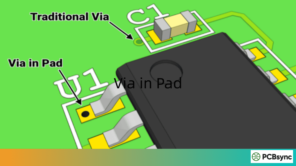
Via in pad is a PCB design technique where you place a via directly within the copper landing pad of a surface-mount component, rather than routing a trace away from the pad to a separate via location.
In traditional PCB design, we use what’s called “dog-bone” fanout — a short trace connecting the component pad to a nearby via. This works fine for larger pitch components, but becomes impossible when you’re dealing with fine-pitch BGAs or high-density layouts.
With via in pad (also called VIP, VIPPO, or POFV), the via sits right inside the pad itself. The via is then filled with epoxy resin, planarized to create a flat surface, and plated over with copper. This gives you a smooth, solderable surface that looks and functions just like a regular pad.
Before we dive deeper, let’s clear up some terminology confusion that I see all the time:
Via in Pad (VIP): The general technique of placing vias inside component pads
VIPPO (Via in Pad Plated Over): VIP with epoxy fill and copper cap plating — the most common implementation
POFV (Plated Over Filled Via): Same as VIPPO, just different terminology some fabs use
Filled and Capped Via: Another way of describing the VIPPO process
In practice, when someone says “via in pad,” they almost always mean the filled and plated-over version. Open vias in pads (without fill) create too many assembly problems to be practical for production.
Here’s the honest truth: via in pad isn’t for every design. I’ve seen engineers use it when they didn’t need to, adding unnecessary cost and complexity. Let me break down the real scenarios where VIP becomes essential.
1. Fine-Pitch BGA Components (≤0.5mm Pitch)
This is the most common reason you’ll reach for via in pad. When BGA ball pitch drops below 0.5mm, there simply isn’t enough space between pads for traditional dog-bone fanout. The math doesn’t work — you can’t fit a via with proper annular ring plus routing clearance in that tiny gap.
Rule of thumb: If your BGA pitch is 0.8mm or larger, you can usually get away with dog-bone routing. At 0.65mm, it gets tight but might still work. Below 0.5mm? Via in pad is your only realistic option.
2. High-Density Interconnect (HDI) PCBs
When every square millimeter counts and you’re stacking components as densely as possible, via in pad lets you reclaim the space that would otherwise go to fanout traces. This is especially critical in:
Smartphones and wearables
Medical implants
Aerospace and defense electronics
High-performance computing modules
In HDI designs, you’re often already paying for advanced processes like laser drilling and sequential lamination. Adding via in pad becomes a marginal cost increase rather than a major line item. If you’re building any HDI board with microvias, you should seriously evaluate whether via in pad makes sense for your BGA routing.
I worked on a wearable device last year where the client insisted on a board size smaller than what seemed physically possible. The only way we made it work was combining via in pad with stacked microvias and a 10-layer HDI stackup. Without VIP technology, we would have needed at least 30% more board area just for escape routing.
3. Thermal Management Requirements
Some components have exposed thermal pads that need vias to transfer heat to inner copper planes. Thermal vias placed directly in the pad provide a more efficient heat dissipation path than routing around the pad.
This is particularly relevant for:
QFN and QFP packages with exposed thermal pads (e-pads)
Power MOSFETs and voltage regulators in D2PAK or similar packages
LED driver ICs that need to dissipate significant heat
High-power processors with thermal interface pads
For thermal via in pad applications, you have some flexibility. Because the thermal pad is relatively large compared to fine-pitch BGA pads, you can often use larger vias (0.3-0.4mm) that are easier to fill reliably. The thermal pad area is also typically large enough that you won’t have solder starvation issues even with multiple vias.
One important consideration: thermal vias in pad may not always require the full VIPPO treatment. If the via is covered by the component’s thermal pad and you’re using paste-in-hole reflow, you might be able to use simpler processing. But this needs to be coordinated carefully with your assembly house.
4. High-Speed Signal Integrity
Shorter signal paths mean lower parasitic inductance and capacitance. For high-frequency designs where every millimeter of trace length matters, via in pad can improve signal integrity by eliminating the dog-bone trace entirely.
Consider the math: A typical dog-bone fanout adds 0.5-1.0mm of trace length per via transition. For a DDR4 or DDR5 memory interface with hundreds of signals, that’s significant cumulative inductance. Via in pad removes this entirely, giving you cleaner transitions.
High-speed applications where via in pad provides measurable benefits include:
For these applications, the performance improvement from via in pad often justifies the additional cost. When you’re spending thousands of dollars on high-speed simulation tools to optimize timing, saving a few dollars per board by avoiding VIP doesn’t make much sense.
5. Decoupling Capacitor Placement
When you need bypass capacitors as close as possible to BGA power pins, via in pad allows you to place capacitors directly on the back side without competing for routing space with escape vias.
The traditional approach creates a conflict: you need vias to escape BGA signals, but those same vias block capacitor placement on layer 2 or the bottom side. Via in pad solves this elegantly — the vias go through the BGA pads themselves, leaving the space between pads available for capacitor mounting vias.
For high-performance FPGAs and processors that demand extensive power decoupling, this can be the deciding factor for via in pad adoption. Without it, achieving proper PDN (power delivery network) impedance becomes extremely difficult.
After implementing VIP in dozens of designs, here’s what I’ve found are the real, practical benefits:
Space Efficiency
By eliminating dog-bone fanout, you can reduce your board size or fit more functionality into the same footprint. In one recent project, switching to via in pad let us shrink a 4-layer board to what would have otherwise required 6 layers.
Improved Signal Performance
Shorter paths from the BGA ball to the inner layer trace means:
Lower parasitic inductance (critical for power delivery networks)
Filled vias under thermal pads create efficient heat transfer channels to inner copper planes or the opposite side of the board. For power devices, this can make the difference between reliable operation and thermal failure.
Simplified BGA Escape Routing
Complex BGAs with hundreds of pins become much more manageable when you can drop vias directly through the pads. What would require multiple routing layers with dog-bone fanout might only need two layers with via in pad.
Disadvantages and Challenges
Let’s be real about the downsides — because ignoring them will bite you during PCB manufacturing or assembly.
Higher Manufacturing Cost
Via in pad adds 8-10 extra steps to the fabrication process. Expect a cost increase of 15-25% compared to standard boards. For prototypes, this might not matter much. For production runs of thousands of units, it adds up quickly.
Longer Lead Times
Those extra manufacturing steps take time. Your standard 5-day turn becomes 7-10 days. Plan accordingly.
Potential Reliability Concerns
If the via fill isn’t done properly, you risk:
Solder wicking: Solder flows into unfilled vias instead of forming proper joints
Outgassing: Trapped air in poorly filled vias expands during reflow, causing voids
CTE mismatch: Epoxy expanding at different rates than surrounding laminate can cause stress cracks
Design Complexity
You need to understand IPC annular ring requirements, work with your fab house on their capabilities, and properly call out via in pad in your fabrication notes. It’s not something you can just drop into a design without thought.
Via in Pad Design Guidelines
Getting via in pad right requires attention to specific design parameters. Here are the guidelines I follow:
Via Sizing Parameters
Parameter
Recommended Value
Notes
Via Diameter (Finished Hole)
0.15-0.25mm
Smaller for fine-pitch, larger for thermal
Pad Diameter
Via diameter + 0.20-0.30mm
Must meet IPC annular ring requirements
Annular Ring
0.10-0.15mm minimum
Check your fab’s Class 2/3 capabilities
Drill Size
Finished hole + 0.05mm
Account for plating
Aspect Ratio
≤12:1
Lower is better for reliable filling
BGA Fanout Parameters
For BGA via in pad designs specifically:
BGA Pitch
Via Hole Diameter
Trace Width
Annular Ring
0.8mm
0.20mm
4 mil
0.35-0.40mm
0.65mm
0.15-0.18mm
3-4 mil
0.30-0.35mm
0.5mm
0.15mm
3 mil
0.25-0.30mm
0.4mm
0.10-0.15mm
2.5-3 mil
0.20-0.25mm
Fill Material Selection
Fill Type
Cost
Thermal Conductivity
Best For
Non-conductive Epoxy
Lower
Poor
Standard signal routing
Conductive Epoxy (Silver)
5x higher
Good
Thermal vias, high-current
Copper Fill
Highest
Excellent
RF, high-power, HDI stackups
For most designs, non-conductive epoxy fill is the right choice. It’s cost-effective and works fine for signal vias. Reserve conductive fill for specific thermal or high-current applications where the extra cost is justified.
Via in Pad Manufacturing Process
Understanding how your fab house will build this helps you design for manufacturability. Here’s the step-by-step process:
Step 1: Drilling
Vias are drilled directly into the pad locations. For standard via in pad, mechanical drilling works for holes ≥0.15mm. Smaller holes (microvias) require laser drilling.
The drill accuracy becomes critical here because the via must be precisely centered in the pad. Any offset reduces the effective annular ring and can cause failures. Most fabs use vision-aligned drilling systems for via in pad to maintain tight positional tolerances.
Step 2: Copper Plating
The via barrel is plated with copper to establish electrical conductivity between layers. This is standard PTH processing, but the copper thickness must be carefully controlled — typically 20-25μm in the barrel.
For via in pad, the plating uniformity matters more than for traditional vias because any irregularity affects the subsequent filling and planarization steps.
Step 3: Via Filling
The via hole is filled with epoxy resin (conductive or non-conductive). This is typically done using a screen printing or vacuum process to ensure complete fill without voids.
The filling process is where quality really matters. Poor filling leads to:
Air pockets that cause outgassing during reflow
Incomplete fill that creates surface depression
Contamination that affects adhesion of the cap plating
Quality fab houses use automated fill inspection (often with X-ray) to verify complete via filling before proceeding.
Step 4: Planarization
The filled via surface is ground flat to be coplanar with the surrounding copper. Any bump or depression will cause soldering problems.
This step requires precision grinding equipment. The surface must be flat to within ±12.5μm (0.5 mil) to meet typical requirements. Some high-reliability applications specify tighter tolerances.
Step 5: Cap Plating
A final copper layer is electroplated over the filled via, creating a continuous, flat pad surface. Typical cap copper thickness is 1 mil (25μm) minimum.
The cap plating must bond well to both the surrounding copper and the filled via material. Proper surface preparation between steps is essential.
Step 6: Surface Finish
Standard surface finish (ENIG, HASL, OSP, etc.) is applied just like any other pad. The filled and capped via becomes indistinguishable from a solid copper pad at this point.
Cost Drivers in Manufacturing
Understanding what drives via in pad cost helps you optimize your design:
Cost Factor
Impact
How to Minimize
Via Count
High — each via requires filling
Only use VIP where necessary
Via Size
Medium — larger vias need more fill material
Use smallest size that meets requirements
Fill Type
High — conductive fill costs 5x more
Use non-conductive unless thermal/current demands
Aspect Ratio
Medium — high ratios harder to fill
Keep below 10:1 when possible
Quantity
Lower at volume
Negotiate pricing for production runs
Via in Pad vs Dog-Bone Fanout: Decision Guide
Still not sure which approach is right for your design? Here’s my decision flowchart:
Use Dog-Bone Fanout When:
BGA pitch is 0.8mm or larger
Board space isn’t severely constrained
Budget is tight (especially for production)
Standard lead times are acceptable
Signal integrity requirements aren’t extreme
Your fab house has limited VIP capabilities
It’s a prototype with uncertain production volumes
Use Via in Pad When:
BGA pitch is 0.5mm or smaller
You’re out of routing channels
Thermal performance is critical
High-speed signal integrity demands shortest paths
HDI/miniaturization is a primary goal
You’re already using HDI processes (adds marginal cost)
Production volumes justify the tooling investment
Component datasheets specifically recommend VIP
Real-World Decision Example
Let me walk through a recent design decision I made. The project had:
An FPGA with 0.8mm pitch BGA (484 balls)
DDR3 memory with 0.8mm pitch BGAs
A processor with 0.65mm pitch BGA (324 balls)
Target board size: 100mm x 80mm
Analysis:
The FPGA and memory could use dog-bone fanout — 0.8mm pitch gives enough room, and they weren’t in the critical timing path. But the processor at 0.65mm was borderline. I did the math:
Available space between pads: 0.65mm – pad diameter (~0.35mm) = 0.30mm
Minimum via diameter: 0.2mm
Annular ring needed: 0.1mm each side
Total via pad required: 0.4mm
It wouldn’t fit with standard routing. Via in pad was required for the processor but not the FPGA or memory.
Result: We used via in pad only on the processor, keeping costs reasonable while solving the routing challenge. Mixed approaches like this are common in practice.
Hybrid Approach: Selective Via in Pad
You don’t have to go all-or-nothing. Many successful designs use via in pad selectively:
VIP for fine-pitch components only
Dog-bone for larger-pitch components
VIP for signal pins, dog-bone for power/ground (where inductance matters less)
VIP for the BGA inner rings, dog-bone for outer rings that have escape room
This hybrid approach optimizes cost while solving the specific routing challenges that demand via in pad technology.
Common Via in Pad Mistakes to Avoid
I’ve learned these lessons the hard way so you don’t have to:
Mistake 1: Not Specifying Fill in Fab Notes
If you don’t explicitly call out via in pad with fill requirements, your fab house might just deliver open vias in pads. Your assembler will then refuse to run the board, or worse, you’ll get solder-starved joints.
Solution: Add clear fab notes: “Via in pad on all BGA pads. Fill with non-conductive epoxy, planarize, and plate over. Via fill per IPC-4761 Type VII.”
Mistake 2: Ignoring Fab Capabilities
Not every PCB manufacturer can do via in pad well. Some can’t handle it at all. Others have minimum via sizes or aspect ratios that might not work for your design.
Solution: Confirm capabilities before finalizing your design. Send your stackup and via requirements for a DFM review.
Mistake 3: Mixing VIPPO and Open Vias in Same Pad
Sometimes designers leave some vias in a BGA pattern unfilled while filling others. This creates assembly problems because solder behaves differently on filled versus open vias.
Solution: Be consistent. Fill all vias in pad, or use dog-bone for all.
Mistake 4: Insufficient Annular Ring
Cramming the biggest possible via into a tiny pad might seem like good thermal design, but if your annular ring is too small, you’ll fail IPC requirements and possibly have reliability issues.
Solution: Calculate annular ring properly. For Class 2: minimum 0.05mm. For Class 3: minimum 0.075mm. Include drill tolerance in your calculation.
Mistake 5: Forgetting Thermal Expansion
Epoxy fill has a different coefficient of thermal expansion (CTE) than the surrounding FR-4 laminate and copper. Over repeated thermal cycles, this mismatch can cause cracking.
Solution: Use high-quality epoxy fills with CTE matched to your laminate. For high-reliability applications, consider copper fill.
Useful Resources and Tools
Here are resources I regularly use for via in pad designs:
Design Standards and Guidelines
IPC-4761: Covers via fill and protection types (Types I-VII) — essential reading for understanding fill options
IPC-2221: General PCB design standard including via requirements
IPC-6012: Qualification and performance specification for rigid PCBs
IPC-7095: BGA design and assembly process guidance
JEDEC standards: Ball pitch and package dimensions for standard BGAs
Huaqiu DFM: Free DFM analysis software that detects via in pad requirements and flags potential issues
Altium Designer: Has built-in via in pad design rules and constraint management
Cadence OrCAD/Allegro: Supports VIPPO design rule checks and padstack definitions
KiCad 7+: Via in pad support with improved pad stack editing
Siemens Xpedition: Enterprise-level via in pad design and analysis
Online Calculators and Tools
Saturn PCB Toolkit: Free calculator for via current capacity and thermal resistance
Polar SI9000: Impedance and via modeling for signal integrity
Fab house DFM tools: Most major fabs offer online DFM checking
Via aspect ratio calculators: Available on most fab websites
Recommended Reading
For those wanting to go deeper on via in pad and HDI technology:
“High Speed Digital Design: A Handbook of Black Magic” by Howard Johnson — foundational for understanding why VIP matters for signal integrity
“HDI Handbook” by Happy Holden — comprehensive guide to HDI technologies including via in pad
IPC APEX conference proceedings — latest research on via filling and reliability
Component Manufacturer Resources
Many semiconductor companies provide specific guidance on via in pad for their packages:
Intel FPGA (formerly Altera): Package-specific layout guides with VIP recommendations
AMD/Xilinx: Detailed BGA breakout guidance including via in pad rules
Texas Instruments: Power pad thermal via guidelines
NXP/Freescale: BGA routing application notes
Microchip: Package landing pattern guidelines
Frequently Asked Questions About Via in Pad
How much does via in pad add to PCB cost?
Via in pad typically increases fabrication cost by 15-25% compared to standard processing. The exact amount depends on via count, hole sizes, and your fab house’s pricing structure. For high-volume production, negotiate pricing — the per-unit cost impact decreases at scale.
Can I use via in pad on a 2-layer board?
Technically yes, but it’s rarely practical. Via in pad is most valuable for routing between layers in dense designs. On a 2-layer board, you usually have enough surface routing space to use traditional vias. The exception might be thermal vias under power components.
What’s the minimum via size for via in pad?
Most PCB manufacturers can handle via in pad down to 0.10mm finished hole with laser drilling for microvias. For mechanically drilled vias, 0.15mm is typically the practical minimum. Always verify with your specific fab house.
Is via in pad the same as VIPPO?
VIPPO stands for “Via in Pad Plated Over” and refers specifically to via in pad with epoxy fill and copper cap plating. Via in pad is the broader term that includes VIPPO. You might also see “POFV” (Plated Over Filled Via) used interchangeably with VIPPO.
Do I need conductive or non-conductive fill?
Non-conductive epoxy fill is the standard choice for most applications. It’s significantly cheaper and works perfectly for signal vias. Use conductive fill (silver epoxy or copper) only when you specifically need enhanced thermal conductivity or are passing significant current through the via. Conductive fill costs approximately 5x more than non-conductive.
Conclusion
Via in pad technology has become essential for modern high-density PCB design. When you’re working with fine-pitch BGAs, tight board spaces, or demanding signal integrity requirements, VIP gives you the routing freedom that traditional dog-bone fanout simply cannot provide.
The key is knowing when to use it. Don’t reach for via in pad just because you can — it adds cost and complexity that isn’t always justified. But when your design truly demands it, understanding the guidelines, working closely with your fabricator, and avoiding common mistakes will help you achieve reliable, manufacturable boards.
If you’re starting a new high-density design, my recommendation is simple: check your BGA pitches first. Anything at 0.5mm or below, plan for via in pad from the beginning. You’ll save yourself the headache of trying to retrofit it later when you realize dog-bone routing just isn’t going to work.
Inquire: Call 0086-755-23203480, or reach out via the form below/your sales contact to discuss our design, manufacturing, and assembly capabilities.
Quote: Email your PCB files to Sales@pcbsync.com (Preferred for large files) or submit online. We will contact you promptly. Please ensure your email is correct.
Notes: For PCB fabrication, we require PCB design file in Gerber RS-274X format (most preferred), *.PCB/DDB (Protel, inform your program version) format or *.BRD (Eagle) format. For PCB assembly, we require PCB design file in above mentioned format, drilling file and BOM. Click to download BOM template To avoid file missing, please include all files into one folder and compress it into .zip or .rar format.


