Inquire: Call 0086-755-23203480, or reach out via the form below/your sales contact to discuss our design, manufacturing, and assembly capabilities.
Quote: Email your PCB files to Sales@pcbsync.com (Preferred for large files) or submit online. We will contact you promptly. Please ensure your email is correct.
Notes: For PCB fabrication, we require PCB design file in Gerber RS-274X format (most preferred), *.PCB/DDB (Protel, inform your program version) format or *.BRD (Eagle) format. For PCB assembly, we require PCB design file in above mentioned format, drilling file and BOM. Click to download BOM template To avoid file missing, please include all files into one folder and compress it into .zip or .rar format.
If you’ve been designing PCBs for any length of time, you’ve probably faced this question: should I tent, plug, or fill my vias? The answer isn’t always straightforward, and picking the wrong via covering method can lead to assembly defects, reliability issues, or unnecessarily inflated costs
I’ve spent years troubleshooting boards where solder wicked down into open vias during reflow, creating dry joints that were nightmares to debug. That experience taught me that via covering isn’t just a checkbox on your fab order—it’s a design decision that affects manufacturability, reliability, and cost.
This guide breaks down everything you need to know about via covering options, from basic tenting to advanced filled-and-capped processes, with practical recommendations based on real-world applications.
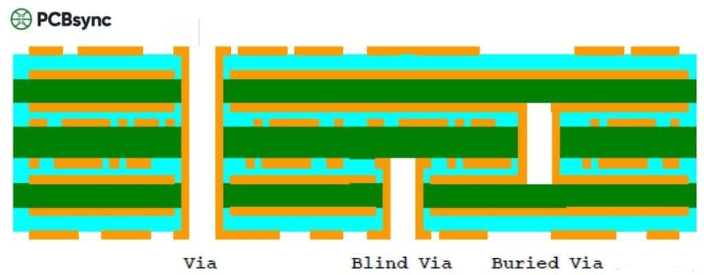
Via covering refers to any method used to protect or seal the via hole on a printed circuit board. A via is essentially a plated-through hole that connects copper traces between different PCB layers. Without protection, these holes remain exposed to the environment and can cause several problems during PCB manufacturing and operation.
When vias are left open (uncovered), they create pathways for solder paste to flow through during assembly. This solder wicking phenomenon pulls paste away from component pads, resulting in insufficient solder joints. Open vias also accumulate flux residue, moisture, and contaminants that can compromise long-term reliability.
Via covering solves these problems by sealing or protecting the via opening using solder mask, epoxy, or conductive materials. The choice of covering method depends on via size, application requirements, and budget constraints.
Why Via Covering Matters
Here’s what can go wrong without proper via covering:
Solder bridging: Exposed vias near SMD pads can cause paste to wick into the hole, creating shorts or weak joints
Contamination: Flux residue and moisture trapped in open vias accelerate corrosion
Short circuits: During wave soldering, solder can travel through open vias and create unwanted connections
Test point accessibility: Once you tent a via, you lose the ability to probe it—sometimes that’s a problem
The IPC-4761 standard (“Design Guide for Protection of Printed Board Via Structures”) defines seven via protection types that have become industry-standard terminology. Understanding these classifications helps you communicate clearly with your fabricator and ensures you get the coverage you actually need.
Types of Via Covering Methods: Complete Breakdown
Let’s walk through each via covering method, from simplest to most complex. I’ll include the IPC-4761 designations where applicable, along with practical guidance on when to use each approach.
1. Untented Vias (Open Vias)
Untented vias have no solder mask coverage—both the annular ring and the via hole remain exposed and receive the same surface finish (HASL, ENIG, etc.) as your solder pads.
When to use untented vias:
You need test points for in-circuit testing or debugging
The design requires heat dissipation through the via barrel
Vias are located far from any SMD pads where solder wicking isn’t a concern
The downsides:
Risk of solder bridging during assembly, especially with vias near BGA or fine-pitch components
Exposed copper oxidizes over time without proper surface finish
Wave soldering can push solder through the hole to the opposite side
Design rule: If using untented vias with HASL finish, maintain at least 0.2mm clearance from other exposed copper to prevent solder bridging during the hot air leveling process.
2. Tented Vias (IPC-4761 Type I & II)
Via tenting is the most common and cost-effective covering method. The via is simply covered with liquid photoimageable (LPI) solder mask during normal solder mask application—no extra process steps required.
Type I-a: Tented on one side only Type I-b: Tented on both sides Type II-a/b: Tented and covered with additional solder mask layer
Via size limitations: Tenting works reliably for vias ≤0.3mm (12 mils) in diameter. Larger vias may not tent completely—the solder mask bridges the opening but can crack or leave pinholes.
The yellowing issue: You’ve probably noticed some tented vias appear yellow or brown. This happens because solder mask is applied as a liquid and heated to flow level. During this process, mask can drain into the via hole, leaving a thinner coating over the annular ring. The copper underneath shows through, creating that discoloration. It’s cosmetic, not a defect.
Best practices for tented vias:
Always tent both sides of through-hole vias to prevent chemical entrapment during manufacturing
Specify via tenting in your fab notes when removing mask clearances from via Gerbers
Tent all vias under QFP and BGA packages to prevent solder wicking
For vias larger than 0.3mm, consider plugging instead of tenting
3. Plugged Vias (IPC-4761 Type III & IV)
Via plugging goes a step further than tenting by partially or fully filling the via hole with non-conductive material (typically solder mask ink or epoxy), then optionally covering with a solder mask layer.
Type III-a/b: Plugged only (one-sided or double-sided) Type IV-a/b: Plugged and covered with solder mask
Via size range: Plugged vias work best for holes between 0.4mm and 0.5mm diameter. Larger holes become difficult to fill completely and may show dimples or voids.
Process considerations:
Plugging uses a screening or vacuum process to force ink into the via barrel before standard solder mask application. Multi-layer PCBs typically use single-sided plugging (Type III-a or IV-a) because double-sided plugging can trap gases that expand during reflow, causing blowouts.
When plugging makes sense:
Vias located within BGA footprints but not directly in pads
Applications requiring complete via sealing for vacuum handling during assembly
Designs where tenting alone can’t reliably close larger via holes
4. Filled Vias (IPC-4761 Type V & VI)
Filled vias take plugging to the extreme—the via barrel is completely filled with non-conductive epoxy or resin. Type VI adds a solder mask covering over the fill material.
Type V: Filled with non-conductive paste (no covering) Type VI-a/b: Filled and covered with solder mask
When filled vias are necessary:
High-reliability applications where zero contamination risk is acceptable
Buried via structures in sequential lamination builds
Boards requiring conformal coating where open vias would trap coating material
Filled vias provide excellent protection but add cost and processing time. For most commercial applications, plugged vias (Type III/IV) offer sufficient protection at lower cost.
5. Filled and Capped Vias (IPC-4761 Type VII)
This is the premium via covering option, used primarily for via-in-pad applications. The process involves:
Filling the via completely with non-conductive (or conductive) paste
Curing the fill material
Planarizing (grinding flat) the via surface
Metallizing and copper plating over the filled via
The result is a flat, solderable surface directly over the via—essential for placing BGA balls or SMD pads directly on via locations.
Two fill material options:
Fill Type
Material
Thermal Conductivity
Best Application
Epoxy-filled
Non-conductive epoxy resin
~0.25 W/mK
Standard via-in-pad
Copper-filled
Conductive copper paste
~8 W/mK
High-power thermal vias
Via-in-pad benefits:
Eliminates dog-bone routing for BGA breakout, increasing routing density
Provides flat pad surface for reliable solder joints
Enables stacked via structures in HDI builds (with caution—see note below)
Important warning: Don’t stack microvias directly on Type VII buried vias. This combination has extremely high failure rates. Stagger the microvia offset from the buried via landing pad.
Getting via covering right requires attention to several design parameters. Here are the key rules to follow:
Via Size Constraints
Tenting: Maximum 0.3mm (12 mil) diameter for reliable mask bridging
Plugging: 0.4mm to 0.5mm diameter optimal range
Filling: Do not exceed 0.5mm—larger holes may show incomplete fill or bubble formation
Spacing Requirements
Maintain minimum 0.35mm clearance between via pad edge and adjacent solder mask openings for plugging
Via-in-pad applications require at least 0.15mm between filled via edge and pad boundary
Keep untented vias at least 0.2mm from other exposed copper when using HASL finish
Fabrication Notes
Always include clear via covering specifications in your fab notes:
Via covering requirements:- All vias ≤0.3mm: Tent both sides with solder mask- Vias 0.3mm-0.5mm in BGA area: Plug with epoxy (Type IV-a)- Via-in-pad locations: Fill and cap per IPC-4761 Type VII- Specify via drill sizes requiring plugging in separate layer
How to Choose the Right Via Covering Method
Selecting the appropriate via covering comes down to answering a few key questions:
1. Where are the vias located?
Under BGA/QFP components → Tent minimum, plug preferred
In the pad → Filled and capped required
Far from components → Untented may be acceptable
2. What’s your via diameter?
≤0.3mm → Tenting works reliably
0.3-0.5mm → Consider plugging
>0.5mm → Plugging/filling not recommended; redesign if coverage needed
3. What’s your reliability requirement?
Consumer electronics → Tenting usually sufficient
Automotive/industrial → Plugging recommended
Medical/aerospace → Filling or filled-and-capped
4. What’s your budget?
Tenting adds zero cost to standard PCB fabrication. Plugging adds moderate cost. Filled-and-capped vias can add significant expense—sometimes 30-50% to via processing costs.
Via Covering in Different PCB Applications
Different applications demand different via covering approaches. Here’s what works best in common scenarios:
Consumer Electronics
For smartphones, tablets, and wearables, board real estate is precious. Via-in-pad with filled-and-capped processing enables the tight BGA fanout these designs require. However, for less dense consumer boards (IoT devices, smart home products), simple tenting keeps costs down while providing adequate protection.
Automotive Electronics
Automotive PCBs face extreme temperature cycling, vibration, and potential exposure to moisture and contaminants. Plugged vias (Type III or IV) are typically the minimum requirement. Critical ECU and safety-system boards often specify filled vias to eliminate any possibility of contamination-related failures over the vehicle’s 15+ year expected lifespan.
Medical Devices
Class II and III medical devices face stringent reliability requirements. Most designs specify filled-and-covered vias (Type VI) minimum, with via-in-pad applications requiring full Type VII processing. Documentation of via covering compliance is often required for regulatory submissions.
Aerospace and Defense
Mil-spec boards typically require via filling per IPC-4761 Type VI or VII, with 100% fill verification through cross-sectioning of test coupons. The additional processing cost is justified by the catastrophic consequences of field failures in these applications.
Common Via Covering Problems and Solutions
Even with proper specification, via covering can go wrong. Here’s what to watch for:
Incomplete Tenting (Pinholes)
Cause: Via too large for reliable mask bridging, or solder mask too thin over via.
Solution: Reduce via diameter below 0.3mm, or upgrade to plugged vias.
Yellowing/Browning of Tented Vias
Cause: Thin solder mask over annular ring allows copper color to show through.
Solution: This is cosmetic only. No action needed unless customer specification prohibits it.
Plugging Voids and Dimples
Cause: Incomplete fill, trapped air during screening process.
Solution: Use vacuum plugging process, verify via diameter within capability limits.
Blowouts During Reflow
Cause: Trapped gases in double-sided plugged vias expanding during soldering heat.
Solution: Use single-sided plugging (Type III-a or IV-a) for multilayer boards.
DFM Considerations for Via Covering
Working with your fabricator early in the design process prevents costly surprises. Here are the key DFM questions to address:
Verify Fabricator Capabilities
Not all PCB manufacturers support all via covering types. Before finalizing your design:
Confirm minimum and maximum via diameters for each covering type
Ask about fill material options (conductive vs. non-conductive)
Verify dimple and planarity specifications for Type VII filled-and-capped vias
Request capability documentation for high-reliability applications
Gerber and Drill File Setup
Proper file preparation ensures your via covering intent translates to the finished board:
For tented vias:
Remove solder mask clearances from the via pads in your Gerber mask layers. Most CAD tools allow you to set “tented” as a via property that automatically removes mask openings.
For plugged/filled vias:
Create a separate drill layer or mechanical layer identifying which vias require plugging or filling. Include specific instructions in your fab notes referencing this layer.
Quality Acceptance Criteria
Define clear acceptance criteria in your purchase order:
Tented vias: No exposed copper on tented side; minor yellowing acceptable
Plugged vias: Minimum 95% fill; no blowouts or voids visible at surface
Filled vias: 100% fill; dimple depth per IPC-6012 Table 3-11
Filled-and-capped: Cap plating thickness ≥5μm; surface depression ≤127μm
What is the difference between via tenting and via plugging?
Via tenting covers only the via opening with solder mask, creating a thin membrane over the hole. Via plugging fills the via barrel partially or completely with non-conductive material before applying solder mask. Plugging provides more reliable sealing but costs more and requires vias within the 0.4-0.5mm range.
What size vias can be reliably tented?
Most fabricators can reliably tent vias with finished hole diameters of 0.3mm (12 mils) or smaller. Larger vias may tent incompletely, leaving pinholes that allow contamination. If your design requires vias larger than 0.3mm under components, consider via plugging instead.
Is via filling necessary for all PCB designs?
No. Via filling (Type V-VII) is typically only necessary for via-in-pad applications, high-reliability products, or designs requiring extremely flat surfaces. For most commercial electronics, tented or plugged vias provide adequate protection at lower cost.
How much does filled-and-capped via processing cost?
Filled-and-capped vias (Type VII) can add 30-50% to your via processing costs compared to standard tented vias. The exact premium depends on via quantity, hole size, and your fabricator’s capabilities. Some manufacturers offer free resin filling for 6+ layer boards as a standard option—worth asking about.
Can I tent vias on only one side of the board?
Yes, single-sided tenting (Type I-a) is possible and sometimes preferred. For example, you might tent the top side to prevent solder wicking while leaving the bottom open for test probe access. However, single-sided tenting on through-hole vias can trap chemicals during manufacturing, potentially causing reliability issues. Double-sided tenting is generally recommended.
Final Thoughts
Via covering might seem like a minor detail in PCB design, but getting it wrong creates headaches that ripple through assembly, test, and field reliability. The good news is that the decision framework is straightforward:
Small vias under components: Tent them
Medium vias in critical areas: Plug them
Vias in pads: Fill and cap them
Vias you need to probe: Leave them open
Specify your requirements clearly in fabrication notes, verify your fabricator’s capabilities before finalizing the design, and don’t be afraid to ask questions. A five-minute conversation with your fab house can prevent weeks of troubleshooting bad solder joints.
The IPC-4761 standard gives you a common language to communicate via covering requirements precisely. Use it, and you’ll spend less time debugging assembly issues and more time designing your next board.
Inquire: Call 0086-755-23203480, or reach out via the form below/your sales contact to discuss our design, manufacturing, and assembly capabilities.
Quote: Email your PCB files to Sales@pcbsync.com (Preferred for large files) or submit online. We will contact you promptly. Please ensure your email is correct.
Notes: For PCB fabrication, we require PCB design file in Gerber RS-274X format (most preferred), *.PCB/DDB (Protel, inform your program version) format or *.BRD (Eagle) format. For PCB assembly, we require PCB design file in above mentioned format, drilling file and BOM. Click to download BOM template To avoid file missing, please include all files into one folder and compress it into .zip or .rar format.


