Inquire: Call 0086-755-23203480, or reach out via the form below/your sales contact to discuss our design, manufacturing, and assembly capabilities.
Quote: Email your PCB files to Sales@pcbsync.com (Preferred for large files) or submit online. We will contact you promptly. Please ensure your email is correct.
Notes: For PCB fabrication, we require PCB design file in Gerber RS-274X format (most preferred), *.PCB/DDB (Protel, inform your program version) format or *.BRD (Eagle) format. For PCB assembly, we require PCB design file in above mentioned format, drilling file and BOM. Click to download BOM template To avoid file missing, please include all files into one folder and compress it into .zip or .rar format.
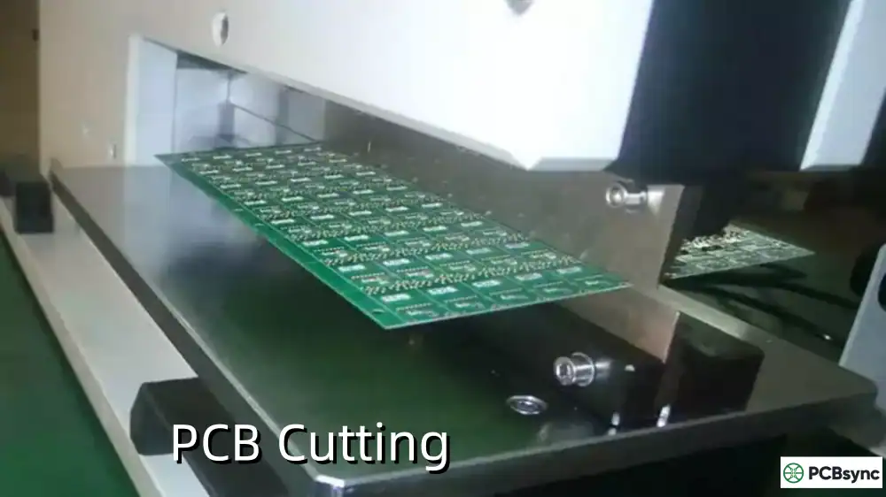
If you’ve ever held a freshly assembled PCB panel in your hands and wondered how to separate those boards without cracking solder joints or damaging components, you’re in the right place. After 15 years designing and manufacturing circuit boards, I’ve seen every depaneling disaster imaginable—from shattered ceramics to stress-cracked BGAs. This guide breaks down the four major depaneling methods so you can pick the right one for your next project.
Quick answer: V-Scoring works best for high-volume rectangular boards. Mouse Bites suit irregular shapes and prototypes. Tab Routing handles complex outlines with edge components. Milling delivers the lowest stress for sensitive assemblies. Most production panels use a combination of methods.
PCB depaneling (also called singulation) is the process of separating individual circuit boards from a larger manufacturing panel. During fabrication and assembly, multiple PCBs are arranged on a single panel to improve efficiency and reduce costs. Once assembly is complete, these boards need to be separated—and this is where method selection becomes critical.
The wrong depaneling method can introduce mechanical stress that damages components, cracks solder joints, or causes latent failures that show up months later in the field. I’ve seen entire production runs scrapped because someone chose V-Scoring for a board with edge-mounted BGAs.
Key Factors in Choosing a Depaneling Method
Before diving into each method, consider these decision factors:
Board shape: Rectangular vs. irregular outlines
Component placement: How close are parts to the board edge?
Production volume: Prototype vs. high-volume manufacturing
Stress sensitivity: Are there fragile components like ceramic capacitors or fine-pitch BGAs?
Edge quality requirements: Does the final product need smooth edges?
Cost constraints: Tooling costs vs. per-unit processing costs
V-Scoring: The Workhorse of High-Volume Production
V-Scoring (also called V-Cut or V-Groove) is the most common depaneling method in the industry. It involves cutting V-shaped grooves into both the top and bottom surfaces of the PCB panel, creating a weakened line where boards can be easily separated.
How V-Scoring Works
A specialized scoring machine uses two rotating blades positioned point-to-point—one above and one below the panel. As the PCB passes between the blades, they cut V-shaped grooves at the predetermined separation lines. The standard approach removes approximately one-third of the board thickness from each side, leaving one-third as a connecting web.
V-Scoring Design Specifications
Parameter
Specification
Notes
V-Groove Angle
20°, 30°, 45°, or 60°
30° is most common
Residual Thickness
0.3mm–1.0mm
Typically 1/3 of board thickness
Minimum Board Thickness
0.6mm (0.8mm recommended)
Thinner boards risk breakage
Residual Thickness Tolerance
±0.1mm
Per IPC-6012E standards
Blade Alignment Tolerance
±0.05mm
Critical for clean breaks
Component Clearance
1mm minimum from V-groove edge
2mm for ceramic capacitors
Maximum Panel Size
600mm × 1200mm
Varies by equipment
Minimum Panel Size
60mm × 45mm
Varies by equipment
When to Use V-Scoring
V-Scoring excels in these scenarios:
Rectangular or square board shapes with straight edges
High-volume production runs (10,000+ units)
Boards where components are at least 1mm from the edge
Projects where processing speed is critical
Cost-sensitive applications where minimal material waste matters
V-Scoring Advantages
Fast processing: Panels pass through the scorer in seconds
Minimal material waste: V-grooves add almost no additional space between boards
Low tooling cost: Standard blades work for most applications
High panel density: More boards fit per panel compared to tab routing
Automated separation: Compatible with automated depaneling equipment
V-Scoring Limitations
Straight lines only: Cannot accommodate curves or complex shapes
Mechanical stress during separation: Breaking the web creates bending stress
Edge quality: May leave slightly rough edges requiring post-processing
Component restrictions: Not suitable for parts hanging over board edges
Panel strength: Deep scores can cause warping in wave soldering
V-Scoring Best Practices
Keep traces 1mm from the V-groove edge to prevent damage during separation
Pull back inner layer planes 1mm from the score line
Use jump scoring on leading/trailing panel edges to prevent sagging in wave solder
Orient chip components parallel to the score line to minimize separation stress
Communicate with your fabricator about V-groove angle requirements
Mouse Bites: Flexibility for Irregular Shapes
Mouse Bites (also called stamp holes or perforated breakaway tabs) use a series of small drilled holes to create a perforated line—similar to the tear-off edge of a postage stamp. After assembly, boards are snapped apart along this perforation.
How Mouse Bites Work
During PCB fabrication, the manufacturer drills a line of small holes (typically 5-8 holes per tab) at strategic locations along the board outline. These holes are positioned close together, leaving only thin strips of material between them. When force is applied, the board breaks cleanly along the perforation, leaving small nubs that can be filed smooth if needed.
Mouse Bites Design Specifications
Parameter
Specification
Notes
Hole Diameter
0.5mm–1.0mm
0.5mm (0.020″) standard
Hole Spacing
0.35mm–0.4mm edge-to-edge
Minimum 0.3mm for strength
Holes Per Tab
5–8 holes
5 holes minimum recommended
Tab Spacing
60mm–90mm apart
77mm center-to-center recommended
Component Clearance
2mm minimum
3mm for sensitive parts
Panel Spacing
1.6mm–2.0mm
Minimum 1.2mm
Board-to-Rail Distance
Mouse bites on one side only
Two sides for board-to-board connections
When to Use Mouse Bites
Mouse Bites are ideal for:
Irregularly shaped or round PCB outlines
Low-to-medium volume production
Prototype runs and hand assembly
Boards that need flexibility in panelization
Projects where V-Scoring isn’t feasible due to shape
Mouse Bites Advantages
Shape flexibility: Works with any board outline—circular, curved, or complex
Low tooling cost: Uses standard CNC drill bits, no special equipment needed
Easy hand separation: Boards snap apart with minimal tools
Compatible with routing: Often combined with tab routing for best results
No specialized equipment: Can be separated manually or with basic tools
Mouse Bites Limitations
Rough edges: Leaves visible “bite marks” requiring filing or sanding
Panel space consumption: Tabs require additional clearance between boards
Weaker than V-Scoring: May break prematurely during handling
Post-processing: Edge cleanup adds labor time
Not ideal for cosmetic products: Visible edge imperfections
Mouse Bites Best Practices
Use staggered hole patterns for more predictable breaks
Place mouse bites in blank areas away from traces and vias
Add at least 2 tab sets per board edge for boards up to 30mm wide
Maintain 0.125″ clearance from mouse bites to nearby components
Consider board thickness: Thicker boards may need larger holes or wider spacing
Tab Routing (also called route and retain) combines CNC routing of the board outline with small connecting tabs that hold boards in place during assembly. These tabs—often reinforced with mouse bites—are removed during depaneling.
How Tab Routing Works
A CNC router mills around the entire PCB outline, leaving only small tabs (typically 3mm wide) to connect the board to the panel frame. These tabs can be solid or perforated with mouse bites for easier separation. After assembly, boards are removed by breaking the tabs or re-routing them with a depaneling router.
Milling or router depaneling uses a high-speed CNC router to completely cut boards from the panel—either by removing tabs or performing a full cut-out. This method generates the lowest mechanical stress of any depaneling technique.
How Milling Depaneling Works
A precision CNC router with a high-speed spindle (30,000–60,000 RPM) follows programmed cutting paths to separate boards from the panel. The router bit mills through the connecting material without bending or flexing the PCB, eliminating the mechanical stress associated with breaking or snapping boards apart.
Milling Equipment Specifications
Parameter
Specification
Notes
Spindle Speed
30,000–60,000 RPM
Higher speed = cleaner cut
Router Bit Diameter
1.0mm–2.0mm
1.2mm common
Feed Rate
15–100mm/sec
Material dependent
Cutting Accuracy
±0.02mm
High precision capability
Positioning Accuracy
±0.02mm
CCD vision alignment common
PCB Thickness Range
0.4mm–3.0mm
Equipment dependent
Typical Cutting Stress
<500 µε (microstrain)
Lowest of all methods
Stress Comparison: Milling vs Other Methods
Research data from strain gauge testing shows significant differences in mechanical stress across depaneling methods:
Depaneling Method
Stress Level (Parallel to Cut)
Stress Level (Perpendicular to Cut)
Router/Milling
Lowest
Lowest
Die Cutting
Low-Medium
Medium
V-Score Rolling Blade
High
Highest
Hand Breaking
Very High
Very High
Source: Strain gauge measurements on 1.2mm FR4 PCB samples
When to Use Milling Depaneling
Milling is the preferred method for:
High-density boards with components near the edge
Assemblies with stress-sensitive components (ceramic caps, BGAs)
Medical, aerospace, and automotive reliability requirements
Complex board shapes requiring full cut-out
Applications where zero mechanical stress is mandatory
Milling Advantages
Lowest mechanical stress: Eliminates bending stress on components and solder joints
Shape flexibility: Cuts curves, radii, and complex outlines
Consistent results: Automated process ensures repeatability
Non-linear cutting: Handles any geometry unlike V-Scoring
Milling Limitations
Equipment cost: CNC routers represent significant capital investment
Slower than V-Score: Processing time is longer per panel
Dust generation: Requires effective vacuum extraction system
Bit wear: Router bits need regular replacement
Not ideal for thin/flexible boards: Better suited for rigid PCBs
Heat generation: High-speed routing may require process control
Milling Best Practices
Use vacuum fixturing to secure boards and prevent movement
Implement dust extraction at the cutting point for cleanliness
Monitor bit wear and replace before precision degrades
Program optimal feed rates based on board material and thickness
Use vision alignment for maximum positional accuracy
Advanced Milling Techniques and Considerations
Inline vs Offline Router Systems
Production environments typically choose between two router configurations:
Inline Routers integrate directly into the SMT production line, depaneling boards immediately after assembly. These systems offer:
Continuous flow production without operator intervention
Reduced handling and potential for damage
Higher initial investment but lower per-unit labor costs
Best for high-volume, dedicated product lines
Offline Routers operate as standalone stations where panels are manually loaded and unloaded:
Lower capital investment
Flexibility to handle multiple product types
Better for low-to-medium volume or high-mix production
Easier to implement quality checks between stages
Vision Alignment Systems
Modern router depaneling machines use CCD camera systems to:
Automatically locate fiducial marks on each panel
Compensate for panel registration errors
Adjust cutting paths in real-time
Achieve positioning accuracy of ±0.02mm
This vision-based alignment is critical when cutting close to components or when panel-to-panel variation exists.
Dust Control and Contamination Prevention
Router depaneling generates significant FR4 dust that can:
Contaminate sensitive components
Create electrical shorts
Pose health hazards to operators
Accumulate in equipment causing maintenance issues
Effective dust management requires:
Vacuum extraction at the cutting point
ESD-safe vacuum systems to prevent static discharge
Regular filter maintenance
Ion air guns to remove residual particles from finished boards
Complete Comparison: V-Scoring vs Mouse Bites vs Tab Routing vs Milling
Criteria
V-Scoring
Mouse Bites
Tab Routing
Milling
Board Shapes
Rectangular only
Any shape
Any shape
Any shape
Edge Quality
Rough
Rough (nubs)
Smooth
Smooth
Mechanical Stress
Medium-High
Medium
Low-Medium
Lowest
Processing Speed
Fastest
Medium
Slow
Medium-Slow
Tooling Cost
Low
Low
Medium
High
Panel Utilization
Highest
Medium
Lower
Medium
Edge Components
Not suitable
Limited
Suitable
Suitable
Production Volume
High volume
Low-Medium
Medium
Medium-High
Post-Processing
Minimal
Filing needed
Minimal
None
Equipment Cost
Low
Low
Medium
High
Dust Generation
None
None
High
High
Best For
Simple, high-volume boards
Prototypes, irregular shapes
Complex shapes, edge parts
Sensitive assemblies
Hybrid Approaches: Combining Depaneling Methods
In real-world production, many panels use multiple depaneling methods to optimize results. Common combinations include:
V-Scoring + Tab Routing
V-Score the straight edges
Tab route the irregular sections
Best of both worlds for mixed geometry
Tab Routing + Mouse Bites
Route the board outline
Add mouse bite perforations to tabs for easy hand separation
Ideal for prototype and low-volume production
V-Scoring + Mouse Bites
V-Score the main panel breaks
Add mouse bites for internal board-to-board connections
Good for maximizing panel density with some shape flexibility
How to Choose the Right Depaneling Method
Use this decision flow to select the optimal method for your project:
Step 1: Board Shape
Rectangular with straight edges → Consider V-Scoring
Irregular, round, or complex → Go to Step 2
Step 2: Edge Components
Components overhanging edges → Tab Routing or Milling
No edge components → Go to Step 3
Step 3: Stress Sensitivity
Ceramic capacitors, fine-pitch BGAs near edge → Milling
Standard components with 2mm+ clearance → Go to Step 4
Step 4: Production Volume
High volume (10,000+) → V-Scoring (if shape allows) or Milling
Low-medium volume → Mouse Bites or Tab Routing
Step 5: Edge Quality Requirements
Cosmetic/precision edges needed → Tab Routing or Milling
Edge quality not critical → V-Scoring or Mouse Bites
Cost Analysis: Understanding the True Cost of Each Method
When evaluating depaneling methods, consider both direct and indirect costs:
Direct Costs
Cost Factor
V-Scoring
Mouse Bites
Tab Routing
Milling
Equipment Investment
$5K–$20K
Included in fab
$15K–$50K
$30K–$150K
Tooling Per Panel
~$0.01
$0
~$0.05
~$0.10
Cycle Time (per panel)
5–10 sec
N/A
30–120 sec
20–60 sec
Labor for Separation
Low
Medium
Low–Medium
None
Consumables
Blade sharpening
None
Router bits
Router bits
Hidden Costs to Consider
Scrap rate: Higher stress methods may increase component failures
Rework costs: Damaged boards during separation require repair or replacement
Quality inspection: Some methods require additional edge inspection
Field failures: Latent stress damage can cause warranty returns
Panel efficiency: Methods requiring more spacing reduce boards per panel
Total Cost of Ownership Example
For a production run of 100,000 boards:
V-Scoring might cost $0.02/board but risk 0.5% stress-related failures
Milling might cost $0.08/board but reduce failures to 0.05%
If each field failure costs $50 in warranty service, milling could save $22,500 despite higher upfront costs
Useful Resources and Tools
IPC Standards for PCB Depaneling
IPC-2221: Generic Standard on Printed Board Design
IPC-6012E: Qualification and Performance Specification for Rigid PCBs
IPC-7351: Generic Requirements for Surface Mount Design
Design Software with Panelization Support
Altium Designer (Embedded Board Array tool)
KiCad (KiKit plugin for panelization)
Eagle (ULP scripts for panelization)
OrCAD PCB Designer
Online Panelization Tools
Most major PCB manufacturers offer free online panelization tools:
JLCPCB Panel Builder
PCBWay Panelization Service
Eurocircuits Panel Editor
Equipment Manufacturers
V-Score Equipment: Manncorp, Fancort, CAB
Router Depaneling: IPTE, Sayaka, Genitec
Laser Depaneling: LPKF, Coherent, Han’s Laser
Frequently Asked Questions About PCB Depaneling
What is the difference between V-Scoring and Mouse Bites?
V-Scoring cuts V-shaped grooves into the PCB panel to create a weakened breaking line, while Mouse Bites use drilled holes to create a perforation. V-Scoring produces cleaner edges and works only for straight lines, while Mouse Bites accommodate any board shape but leave rough edges requiring post-processing. V-Scoring is faster and wastes less material, making it preferred for high-volume production of rectangular boards.
Can I use V-Scoring for irregularly shaped PCBs?
No. V-Scoring can only create straight-line separations because the scoring blades must travel in a continuous line across the panel. For irregular, curved, or complex board shapes, you need Tab Routing or Mouse Bites. Some manufacturers combine V-Scoring for straight edges with Tab Routing for curved sections on the same panel.
How close can components be to the board edge for each depaneling method?
Component clearance requirements vary by method:
V-Scoring: Minimum 1mm, 2mm recommended for ceramic capacitors
Mouse Bites: Minimum 2mm, 3mm for sensitive components
Tab Routing: Minimum 2-3mm from routed edges
Milling: Can accommodate components as close as 1mm with proper fixturing
Always consult your manufacturer’s DFM guidelines for specific requirements.
Which depaneling method causes the least stress on components?
Milling (router depaneling) generates the lowest mechanical stress because it cuts through material without bending the board. Strain gauge testing shows milling produces stress levels 1/10th of rolling blade V-Score cutters and 1/100th of hand breaking. For assemblies with stress-sensitive components like ceramic capacitors or fine-pitch BGAs near board edges, milling is the safest choice.
Is laser depaneling better than mechanical methods?
Laser depaneling offers the ultimate in precision and zero mechanical stress, but comes with trade-offs. It excels for thin/flexible boards, HDI designs, and applications requiring extreme precision. However, laser systems have higher equipment costs and may be slower for thick FR4 boards. For standard rigid PCB production, mechanical methods like milling often provide the best balance of quality, speed, and cost.
Conclusion
Choosing the right PCB depaneling method isn’t just a PCB manufacturing detail—it directly impacts your product’s reliability and your production costs. V-Scoring remains the go-to choice for high-volume rectangular boards where speed and panel density matter most. Mouse Bites provide flexibility for prototypes and irregular shapes without expensive tooling. Tab Routing handles complex designs with edge components that other methods can’t accommodate. And Milling delivers the lowest-stress separation for your most sensitive assemblies.
In most real-world scenarios, the best approach combines multiple methods on a single panel—V-Score where you can, tab route where you must, and mill when component integrity is paramount.
The key is communicating early with your PCB manufacturer about your specific requirements. Share your board shapes, component placements, and production volumes so they can recommend the optimal panelization strategy. A few hours of upfront planning can save weeks of debugging field failures down the road.
Inquire: Call 0086-755-23203480, or reach out via the form below/your sales contact to discuss our design, manufacturing, and assembly capabilities.
Quote: Email your PCB files to Sales@pcbsync.com (Preferred for large files) or submit online. We will contact you promptly. Please ensure your email is correct.
Notes: For PCB fabrication, we require PCB design file in Gerber RS-274X format (most preferred), *.PCB/DDB (Protel, inform your program version) format or *.BRD (Eagle) format. For PCB assembly, we require PCB design file in above mentioned format, drilling file and BOM. Click to download BOM template To avoid file missing, please include all files into one folder and compress it into .zip or .rar format.


