Inquire: Call 0086-755-23203480, or reach out via the form below/your sales contact to discuss our design, manufacturing, and assembly capabilities.
Quote: Email your PCB files to Sales@pcbsync.com (Preferred for large files) or submit online. We will contact you promptly. Please ensure your email is correct.
Notes: For PCB fabrication, we require PCB design file in Gerber RS-274X format (most preferred), *.PCB/DDB (Protel, inform your program version) format or *.BRD (Eagle) format. For PCB assembly, we require PCB design file in above mentioned format, drilling file and BOM. Click to download BOM template To avoid file missing, please include all files into one folder and compress it into .zip or .rar format.
USB Blaster & ByteBlaster: Complete FPGA Programmer Guide for Intel/Altera
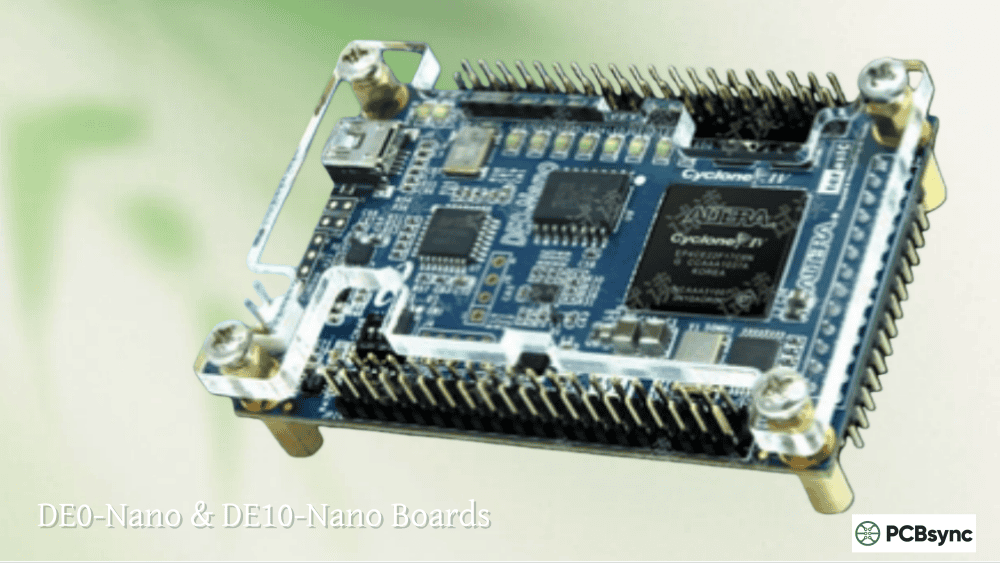
After spending over a decade working with Intel (formerly Altera) FPGAs on everything from prototype boards to production systems, I’ve learned that choosing the right programming cable can make or break your development workflow. Whether you’re setting up your first DE10-Lite board or troubleshooting a stubborn JTAG connection on a custom PCB, understanding the differences between the USB Blaster, USB Blaster II, ByteBlaster, and Ethernet Blaster variants is essential knowledge for any serious FPGA engineer.
This guide cuts through the marketing fluff and gives you the practical, hands-on information you need to select, configure, and troubleshoot Intel FPGA programming cables. I’ll cover everything from pinout specifications and voltage requirements to driver installation gotchas and those frustrating “JTAG chain broken” errors that have cost me countless hours over the years.
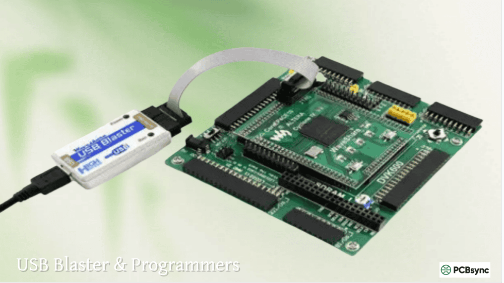
The Intel USB Blaster (also known as the Altera USB Blaster before Intel’s acquisition) is a download cable that interfaces between your PC’s USB port and Intel/Altera FPGA or CPLD devices. It transmits configuration data from Quartus Prime software to the target device through a standard 10-pin header connection.
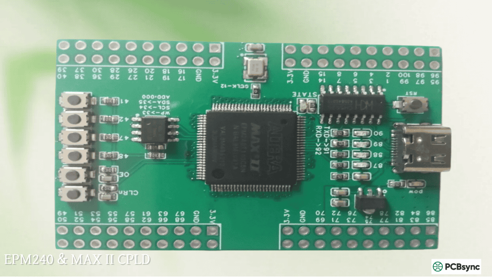
At its core, the USB Blaster is essentially a USB-to-JTAG bridge that converts commands from the Quartus Prime Programmer into the appropriate JTAG signals that FPGAs and CPLDs understand. The original design uses an FTDI FT245 USB controller paired with an Altera CPLD (typically an EPM240 or similar MAX series device) that handles the protocol conversion and signal timing. This clever combination of standard USB interfacing with programmable logic allows the cable to support multiple programming modes: JTAG for most devices, Active Serial (AS) for configuration memories like EPCS and EPCQ devices, and Passive Serial (PS) for certain FPGA families that support serial configuration.
Key Features of the Intel USB Blaster
Supports JTAG, Active Serial (AS), and Passive Serial (PS) programming modes
Compatible with Quartus Prime (Lite, Standard, and Pro editions)
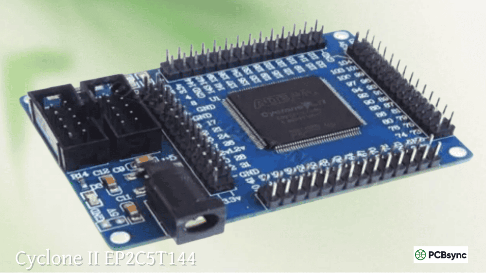
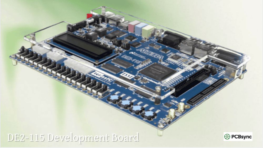
Works with Cyclone, Stratix, Arria, MAX, and legacy FPGA/CPLD families
Supports SignalTap II embedded logic analyzer for real-time debugging
Programs EPCS, EPCQ, and EPC serial configuration devices
Auto-adjusting voltage support from 1.5V to 5.0V (depending on variant)
JTAG clock speeds of 6MHz (USB Blaster I) to 24MHz (USB Blaster II)
USB Blaster I vs USB Blaster II: Which One Do You Need?
One of the most common questions I get from engineers starting with Intel FPGAs is whether they should spring for the USB Blaster II or stick with the cheaper original version. The answer depends on your specific requirements, budget, and target devices.
USB Blaster Comparison Table
Feature
USB Blaster I
USB Blaster II
JTAG Clock Speed
6 MHz
24 MHz (4x faster)
USB Protocol
USB 1.1 Full Speed
USB 2.0 High Speed
Voltage Range
1.5V – 3.3V
1.2V – 5.0V TTL
Memory Speed
Standard
~100x faster (measured)
AES Key Support
No
Yes (secure key programming)
System Console
Limited support
Full parallel interface
Typical Price
$50 – $80 (Terasic)
$199 – $300 (Intel)
In my experience, the USB Blaster II’s biggest advantage isn’t the raw programming speed (though that’s nice) – it’s the System Console integration. When you’re debugging Nios II soft processors or complex Platform Designer systems, the fast parallel interface makes memory reads and register access dramatically faster. If you’re just programming Cyclone or MAX devices and doing occasional SignalTap captures, the original USB Blaster is perfectly adequate.
Altera ByteBlaster and ByteBlaster II: Understanding Legacy Programming Cables
Before USB became ubiquitous, Altera’s primary programming solution was the ByteBlaster series of parallel port cables. While these are largely obsolete today, you might encounter them when working with older equipment or maintaining legacy systems.
ByteBlaster MV vs ByteBlaster II Comparison
The ByteBlaster MV (Multi-Voltage) was Altera’s mid-range parallel port programmer, supporting 3.3V and 5V target systems. The ByteBlaster II added support for even lower voltage devices and improved Active Serial programming capabilities.
Feature
ByteBlaster MV
Altera ByteBlaster II
Interface
25-pin Parallel Port
25-pin Parallel Port
Voltage Support
3.3V, 5.0V
1.8V, 2.5V, 3.3V, 5.0V
EPCS Support
No
Yes (AS mode)
SignalTap II
Limited
Full support
Speed vs USB
~6x slower than USB Blaster
~6x slower than USB Blaster
If you’re still using ByteBlaster cables, it’s probably time to upgrade. Modern PCs rarely have parallel ports, and even USB-to-parallel adapters often don’t work reliably with these cables due to timing requirements. The USB Blaster is approximately six times faster and much more reliable.
Altera Ethernet Blaster: Remote FPGA Programming Solution
The PL-ETH2-BLASTER (Altera Ethernet Blaster II) is a specialized programming cable that connects via standard Ethernet networks instead of USB. This makes it invaluable for certain production and development scenarios.
When to Use the Ethernet Blaster
Remote programming of devices in data centers or distributed systems
Production environments where multiple operators need simultaneous access
Long-distance connections where USB cable length limits (5m) are insufficient
Automated testing systems with network-based control
Situations requiring electrical isolation between programmer and target
The Altera Ethernet Blaster supports both static and dynamic IP addressing via standard TCP/IP protocol, making it easy to integrate into existing network infrastructure. It works with standard CAT 5 UTP cables and supports target voltage levels from 1.2V to 3.3V for modern low-power FPGA families. While more expensive than USB options at approximately $400-500, the remote programming capability becomes essential for certain specialized applications where physical access is impractical or impossible.
FPGA USB Blaster 10-Pin Header Pinout and Connection Details
Getting the physical connections right is critical for reliable FPGA programming operations. The standard Intel/Altera 10-pin JTAG header follows a specific pinout that’s shared across all USB Blaster variants, ByteBlaster cables, Ethernet Blasters, and compatible third-party programmers. Understanding these connections thoroughly will help you design proper JTAG headers on custom PCBs and troubleshoot connection issues efficiently.
Standard 10-Pin JTAG Header Pinout Specification
Pin
Signal Name
Description and Function
1
TCK
Test Clock – JTAG clock signal from programmer to target
2
GND
Ground reference – common return path for all signals
3
TDO
Test Data Out – Data output from target device to programmer
4
VCC(TRGT)
Target voltage sense – determines I/O voltage levels
5
TMS
Test Mode Select – JTAG TAP state machine control
6
nCE / nCS
Chip Enable for AS/PS programming modes (active low)
7
TDI / ASDO
Test Data In (JTAG mode) / AS Data Out (AS mode)
8
nCONFIG
Configuration control for PS mode (active low trigger)
9
DCLK
Data Clock for AS and PS programming modes
10
GND
Ground reference – second ground pin for signal integrity
Critical Design Note: Pin 4 (VCC_TRGT) is the voltage reference pin that the USB Blaster uses to sense target voltage and automatically adjust its I/O signal levels accordingly. The programmer does NOT supply power through this pin – it only measures voltage. Your target FPGA board must be powered separately before connecting the programmer, and the power supply must be stable before attempting any programming operations. Failure to observe this sequence results in “Unable to scan device chain” errors.
PCB Design Considerations for JTAG Headers
When designing custom PCBs with JTAG headers for USB Blaster programming, several important considerations affect reliable operation. The standard 10-pin header uses 0.1″ (2.54mm) pitch with two rows of five pins. Intel recommends using through-hole connectors rather than surface mount headers due to the repeated insertion and removal forces during development. For production fixtures, surface mount headers can work but may have shorter lifetimes.
Signal integrity becomes important at higher JTAG clock speeds. Keep JTAG traces short and avoid routing them near high-speed digital signals or switching power supplies. Pull-up resistors on TCK and TMS (typically 1k to 10k ohms to VCC_TRGT) help ensure clean signal transitions and prevent floating inputs when the programmer is disconnected. Some designs also include a weak pull-down on TDI to ensure defined states during power-up.
Setting Up Intel USB Blaster with Quartus Prime Software
Proper driver installation is typically the first hurdle most engineers face when setting up a new FPGA development environment. The process differs between Windows and Linux operating systems, and there are several gotchas that can waste hours of troubleshooting time if you’re not prepared for them.
Windows USB Blaster Driver Installation Procedure
Connect the USB Blaster to your PC – Windows may show a “Found New Hardware” wizard
Open Device Manager (right-click Start, select Device Manager)
Locate the device under “Other devices” – it may appear as unknown device
Right-click on the device and select “Update Driver Software”
Choose “Browse my computer for driver software”
Navigate to: <Quartus Installation>\drivers\usb-blaster
Select “Include subfolders” checkbox and click Next
Accept security warnings if prompted and complete the installation wizard
Important Driver Location Note: Do NOT select the x32 or x64 subdirectories directly when browsing for drivers. Point to the parent usb-blaster folder and enable “Include subfolders” to let Windows automatically select the appropriate driver version for your operating system architecture. This common mistake causes driver installation failures.
Linux USB Blaster Configuration Steps
Linux requires manual udev rules configuration to grant non-root users access to the USB Blaster hardware. Create a rules file at /etc/udev/rules.d/51-usbblaster.rules containing permissions for the Altera USB device (vendor ID 09fb). After creating the rules file, reload udev with “sudo udevadm control –reload-rules” and reconnect the USB Blaster.
Some Linux distributions (particularly newer versions like Ubuntu 20.04+, Fedora, and Arch) may also require creating a symbolic link for libudev.so. If jtagconfig shows “JTAG chain broken” immediately after connecting a known-good board, try: “sudo ln -s /lib64/libudev.so.1 /lib64/libudev.so.0” and restart the jtagd service.
Configuring Hardware in Quartus Prime Programmer
Launch Quartus Prime and navigate to Tools → Programmer
Click “Hardware Setup” button in the Programmer window toolbar
Select your USB Blaster from the “Currently Selected Hardware” dropdown
Choose the appropriate programming mode (JTAG, Active Serial, or Passive Serial)
Click “Auto Detect” to scan the JTAG chain and identify connected devices
Add your .sof (SRAM) or .pof (flash) file and enable “Program/Configure” checkbox
USB Blaster Clone Options: STM32, CH552, and Third-Party Alternatives
The market is absolutely flooded with inexpensive USB Blaster clones ranging from $3 budget options on AliExpress to $50 branded alternatives on Amazon and electronics distributors. As someone who has tested many of these clones over the years on various FPGA projects, I can tell you there are significant differences in quality, reliability, and compatibility that aren’t obvious from product listings.
Common USB Blaster Clone Implementations
FT245 + CPLD Design (Terasic-style): These clones follow the original Altera reference design closely, using an FTDI FT245 USB chip paired with a small Altera CPLD (typically MAX II EPM240 or similar). They offer the best compatibility and reliability because they match the genuine hardware behavior exactly. The Terasic USB Blaster (UBT) is officially sanctioned by Intel and shares the same USB vendor/product ID as genuine Intel cables.
USB Blaster STM32 Clones: Many of the cheapest clones use an STM32F101 or STM32F103 microcontroller with a 74HC244 octal buffer for level shifting. These are often the most problematic options – the firmware can be buggy, causing Windows blue screens, random programming failures, or JTAG timing issues. Some work fine on Windows but fail mysteriously on Linux due to subtle timing differences in the USB stack.
CH552 Based USB Blaster Clones: A newer generation of budget clones uses the WCH CH552 8051-based USB microcontroller. These are hit-or-miss in terms of compatibility – some work reasonably well, while others have compatibility issues with newer Quartus Prime versions (particularly 23.x and 24.x releases). The CH552 is very inexpensive, which explains their prevalence in the cheapest clones.
PIC18F14K50 Designs: Some hobbyist and DIY designs use Microchip PIC microcontrollers. These typically only support 5V operation and may lack the buffer circuitry needed for lower voltage targets like modern 1.2V or 1.8V FPGA I/O banks. They’re suitable for learning and older devices but problematic for serious development work.
USB ByteBlaster Clone Compatibility Issues and Workarounds
Cheap USB Blaster clones often run the JTAG clock slightly out of specification. The official TCK clock is 6MHz, but some clones run at 12MHz or have significant clock jitter issues due to cheap oscillators or firmware timing problems. This causes intermittent failures with certain FPGA families, particularly newer devices like Arria 10, Cyclone 10, and MAX 10 which have tighter timing requirements than older Cyclone II or III series parts.
If you experience intermittent programming failures with a clone programmer, try these workarounds: shorten the JTAG ribbon cable, add or adjust pull-up resistors on TCK and TMS signals, try a different USB port (particularly USB 2.0 ports rather than USB 3.0), or downgrade to an older Quartus version (18.1 often works better than 23.x or 24.x with problematic clones).
Troubleshooting Common USB Blaster and JTAG Connection Problems
After years of helping engineers debug JTAG issues across dozens of different FPGA projects, I’ve compiled solutions to the most common problems you’ll encounter when using USB Blaster programmers. These troubleshooting steps will help you quickly identify and resolve connection issues.
Fixing “Unable to scan device chain” and “JTAG chain broken” Errors
This is by far the most common error message and can have multiple root causes. Work through these checks systematically:
Verify target board power supply: The FPGA board must be powered and stable before connecting the USB Blaster. The programmer senses voltage through Pin 4 but cannot power the target. Check power LEDs and measure VCC with a multimeter.
Check cable orientation: Pin 1 on the ribbon cable (usually marked with a red stripe or triangle) must align with Pin 1 on the target header. Reversed cables cause immediate failures.
Verify VCC_TRGT voltage: Measure the voltage on Pin 4 of the JTAG header. It should match your FPGA’s JTAG bank voltage (typically 2.5V or 3.3V). Wrong voltage causes I/O level mismatches.
Inspect JTAG signals with oscilloscope: Verify that TCK, TMS, TDI, and TDO have clean edges and proper voltage levels. TCK should show the clock signal during programming attempts.
Check pull-up resistors: TCK and TMS often require pull-up resistors (typically 1k-10k to VCC). Missing or incorrect values cause signal integrity problems and inconsistent detection.
USB Blaster Not Detected in Quartus Prime Programmer
Verify the device appears in Windows Device Manager under “Universal Serial Bus controllers” as “Altera USB-Blaster” (not under Other devices)
If shown under “Other devices” with a yellow warning triangle, the driver needs reinstallation
On Linux systems, check with “lsusb” command for device ID 09fb:6001 (USB Blaster) or 09fb:6010 (USB Blaster II)
Ensure jtagd service is running: execute “jtagconfig” from command line to verify communication
Try a different USB port – some USB 3.0 ports have compatibility issues with USB 1.1 Full Speed devices
Programming Fails at Specific Percentage
If FPGA programming consistently fails at the same percentage point (often around 4% or 25%), this typically indicates a timing or protocol compatibility issue rather than a hardware problem. Try reducing the JTAG clock speed using jtagconfig (available for USB Blaster II), using a genuine programmer instead of a clone, or testing with an older Quartus version. Some cheap clones work reliably with Quartus 18.1 but fail with versions 23.x and 24.x due to protocol changes in the newer JTAG server.
Supported Intel/Altera FPGA and CPLD Device Families
The Intel USB Blaster family supports an extensive range of programmable devices across multiple generations of Intel (formerly Altera) technology. Here’s a comprehensive overview of supported device families.
FPGA Families Supported by USB Blaster
Modern Device Families: Agilex 7, Agilex 5, Stratix 10, Arria 10, Cyclone 10 GX, Cyclone 10 LP, MAX 10
Useful Resources, Downloads, and Documentation Links
Official Intel FPGA Documentation
Intel FPGA Download Cable User Guide (USB Blaster) – UG-USB81204
Intel FPGA Download Cable II User Guide (USB Blaster II)
Programming Cable Driver Information page on Intel FPGA website
Quartus Prime Programmer User Guide – comprehensive programming reference
Software Downloads and Tools
Quartus Prime Lite Edition (Free) – Supports Cyclone IV/V/10 LP, MAX II/V/10
Quartus Prime Standard Edition – Additional device family support
Quartus Prime Pro Edition – Full support for all Intel FPGA devices
USB Blaster Driver Package (included with all Quartus installations)
Third-Party Resources and Community
Terasic USB Blaster Wiki – Detailed troubleshooting guides and FAQs
Intel FPGA Community Forums – Active support from Intel engineers and users
GitHub repositories with USB Blaster clone designs, alternative firmware, and tools
Frequently Asked Questions About Intel USB Blaster Programming
Can the USB Blaster power my FPGA development board?
No, the USB Blaster cannot and should not be used to power your target board. It only senses target voltage through Pin 4 (VCC_TRGT) to automatically set its output I/O levels. Your FPGA board must be powered separately from its own power supply before connecting the programmer. Attempting to power from the USB Blaster will result in “Unable to scan device chain” errors because the voltage sense pin sees 0V without external power.
Is a cheap $5 USB Blaster clone from AliExpress worth buying?
It depends on your use case and tolerance for troubleshooting. For hobby projects with older devices like Cyclone II, Cyclone III, or MAX II CPLDs, cheap STM32-based clones often work adequately. For professional development work or newer device families (Cyclone 10, Arria 10, MAX 10), invest in a genuine Intel or Terasic programmer. The time lost debugging clone-related timing issues and compatibility problems often exceeds the cost savings. If budget is tight, the Terasic USB Blaster (~$50-80) offers genuine compatibility at a reasonable price point.
What’s the maximum cable length I can use with USB Blaster?
The USB specification limits cable length to 5 meters for USB 1.1/2.0 connections without active hubs or repeaters. The JTAG ribbon cable between the USB Blaster dongle and target board should be kept as short as practical – ideally under 15cm (6 inches) for reliable high-speed operation. Long JTAG cables act as antennas and cause significant signal integrity degradation, especially with USB Blaster II running at 24MHz. If you need longer distances, consider the Ethernet Blaster instead.
Can I use USB Blaster with Xilinx or other non-Intel FPGAs?
The standard Intel USB Blaster only works with Intel/Altera devices through Quartus Prime software. The JTAG protocol is standardized, but the programming file formats and device-specific commands are proprietary. For Xilinx devices, use the Xilinx Platform Cable USB or a JTAG-HS3 adapter instead. Some Universal ByteBlaster designs and OpenOCD configurations theoretically support using USB Blaster-compatible hardware with generic JTAG targets, but this is not officially supported and requires significant technical expertise.
Why does my USB Blaster work on Windows but fail on Linux?
This common issue is usually caused by either udev permissions problems (non-root users can’t access USB devices) or library compatibility issues (missing libudev.so symlink). Start troubleshooting by running jtagconfig as root to rule out permissions. If that works, create proper udev rules. If root access still fails, check dmesg for USB enumeration errors. Some cheap clones also have timing issues that are more sensitive under Linux’s USB stack, particularly with modern kernels.
Conclusion: Selecting the Right Intel FPGA Programmer for Your Project
For most engineers working with Intel FPGAs in both professional and hobby contexts, the USB Blaster remains the reliable workhorse programmer of choice. The original USB Blaster (or Terasic UBT equivalent) handles 90% of typical use cases at a reasonable price point and offers excellent compatibility across the full range of Intel/Altera devices. Invest in the more expensive USB Blaster II only if you’re working with Stratix 10, Agilex, or other high-end device families, need AES key programming for design security, or spend significant time debugging with System Console where the faster memory access makes a real difference in your daily productivity.
Avoid the temptation of ultra-cheap USB Blaster clones unless you’re prepared to deal with occasional compatibility headaches and have the technical skills to troubleshoot timing issues. The few dollars saved aren’t worth the frustration when you’re fighting a project deadline and your programmer decides to stop working reliably. When in doubt, the official Intel or Terasic cables provide proven, hassle-free operation across all supported device families and Quartus versions.
Remember: the best FPGA programmer is the one that works reliably every single time you need it, without consuming your valuable engineering time debugging connection problems. Make your selection accordingly based on your specific requirements, budget, and target devices, and enjoy productive FPGA development!
Inquire: Call 0086-755-23203480, or reach out via the form below/your sales contact to discuss our design, manufacturing, and assembly capabilities.
Quote: Email your PCB files to Sales@pcbsync.com (Preferred for large files) or submit online. We will contact you promptly. Please ensure your email is correct.
Notes: For PCB fabrication, we require PCB design file in Gerber RS-274X format (most preferred), *.PCB/DDB (Protel, inform your program version) format or *.BRD (Eagle) format. For PCB assembly, we require PCB design file in above mentioned format, drilling file and BOM. Click to download BOM template To avoid file missing, please include all files into one folder and compress it into .zip or .rar format.


