Inquire: Call 0086-755-23203480, or reach out via the form below/your sales contact to discuss our design, manufacturing, and assembly capabilities.
Quote: Email your PCB files to Sales@pcbsync.com (Preferred for large files) or submit online. We will contact you promptly. Please ensure your email is correct.
Notes: For PCB fabrication, we require PCB design file in Gerber RS-274X format (most preferred), *.PCB/DDB (Protel, inform your program version) format or *.BRD (Eagle) format. For PCB assembly, we require PCB design file in above mentioned format, drilling file and BOM. Click to download BOM template To avoid file missing, please include all files into one folder and compress it into .zip or .rar format.
After spending over a decade working with test engineers and production managers across multiple EMS facilities, I’ve witnessed firsthand the confusion that surrounds PCB testing equipment selection. The choice between a universal tester and a dedicated tester isn’t just a procurement decision—it’s a strategic call that affects your production efficiency, quality metrics, and ultimately your bottom line.
Let me walk you through everything you need to know to make the right choice for your specific manufacturing environment.
A universal tester is a flexible test platform designed to test multiple PCB designs using interchangeable fixtures and reconfigurable test programs. Rather than building a completely new test system for each product, you maintain a single core platform and swap out personality modules or interface adapters to accommodate different board designs.
The concept emerged from the practical challenges faced by contract manufacturers and OEMs producing diverse product portfolios. When your manufacturing floor accumulates dozens of unique test stations—each dedicated to a single product—you’re burning floor space, multiplying maintenance requirements, and creating training nightmares for your operators.
How Universal Testers Work
The architecture of a universal tester typically includes three main elements:
The base platform contains core instrumentation like power supplies, digital multimeters, signal generators, and switching matrices. This equipment remains constant regardless of which product you’re testing. Think of it as your test infrastructure backbone.
The interface system connects the base platform to product-specific fixtures. Mass interconnect systems allow rapid mating with various fixture bases, enabling quick changeovers between products. A technician can typically swap fixtures and be ready to test a different product within minutes rather than hours.
The test program layer contains software routines tailored to each PCB design. While the hardware stays constant, the software defines which measurements to take, what sequences to follow, and what pass/fail criteria to apply. Modern universal test systems run on platforms like NI TestStand, allowing test engineers to develop and maintain programs across the entire product family.
Benefits of Universal Tester Systems
Benefit
Description
Floor Space Optimization
One station replaces multiple dedicated testers
Reduced Changeover Time
Quick fixture swaps vs. complete station moves
Standardized Training
Operators learn one platform for multiple products
Lower Maintenance Costs
Single set of instruments to calibrate and maintain
Future-Proofing
New products integrate with minimal hardware investment
Consistent Documentation
Unified test data formats across product lines
The flexibility factor cannot be overstated. When a customer requests a new product variant or engineering makes a design change, you’re updating a fixture and test program rather than commissioning an entirely new test station.
What is a Dedicated Tester for PCB Assembly?
A dedicated tester is purpose-built for testing a single PCB design or a very narrow family of closely related boards. Every element of the system—the fixture, instrumentation, wiring, and software—is optimized specifically for that product’s test requirements.
Dedicated testers represent the traditional approach to high-volume manufacturing test. When you’re producing 50,000 identical boards per month and the design remains stable for years, the economics favor maximum throughput optimization over flexibility.
How Dedicated Testers Work
A dedicated test system starts with a custom fixture designed around the specific PCB layout. The bed-of-nails fixture contains spring-loaded pogo pins positioned precisely to contact designated test points on the board. Each pin connects directly to the appropriate measurement or stimulus instrument without the switching overhead of a universal system.
The instrumentation package is selected and configured specifically for the product’s test requirements. If the board requires specific analog measurements, high-frequency testing, or boundary scan access, those capabilities are built in without compromises for other products that won’t use them.
Test programs for dedicated systems can be highly optimized because they’re written for a fixed hardware configuration. There’s no abstraction layer for hardware flexibility—just direct, efficient code paths to complete measurements as quickly as possible.
Dedicated Tester Advantages
Advantage
Description
Maximum Throughput
Optimized hardware and software for specific product
Lower Per-Unit Test Cost
Amortized fixture costs across high volumes
Higher Test Coverage
Custom access to all critical test points
Faster Test Cycles
No switching overhead, parallel measurements
Simpler Troubleshooting
Fixed configuration easier to debug
Optimized Reliability
Fewer moving parts, fewer failure modes
For mature products running at volume, dedicated testers can achieve test cycle times that universal systems simply cannot match. When throughput directly impacts your ability to ship product and collect revenue, those seconds per board add up quickly.
Universal Tester vs Dedicated Tester: Head-to-Head Comparison
Choosing between these approaches requires understanding how they compare across the factors that matter most to your operation.
Cost Comparison
Cost Factor
Universal Tester
Dedicated Tester
Initial Platform Investment
$50,000 – $200,000+
$15,000 – $50,000
Per-Product Fixture Cost
$2,000 – $10,000
$5,000 – $25,000
Test Program Development
40-80 hours typical
20-60 hours typical
Floor Space Per Product
Shared (fractional allocation)
Dedicated footprint
Annual Calibration
One set of instruments
One set per station
Maintenance Labor
Consolidated
Distributed
The break-even analysis depends heavily on your product mix. If you’re testing 10+ distinct products at low-to-medium volumes each, universal testing typically wins on total cost of ownership. If you’re testing 2-3 products at very high volumes, dedicated systems usually make more economic sense.
Performance Comparison
Performance Factor
Universal Tester
Dedicated Tester
Typical Test Cycle Time
30-120 seconds
15-45 seconds
Changeover Time
5-30 minutes
Not applicable
Test Point Accessibility
Good (standard pitch)
Excellent (custom design)
Measurement Accuracy
High
Very High
Throughput Capacity
Medium
High
First Pass Yield Impact
Standard
Optimized
Test cycle time differences stem from hardware architecture. Universal systems require switching to route signals between instruments and test points, adding latency. Dedicated systems make direct connections, eliminating this overhead.
Flexibility and Scalability
Factor
Universal Tester
Dedicated Tester
New Product Introduction
2-4 weeks typical
4-8 weeks typical
Design Change Response
Fast (fixture/program update)
Slow (possible fixture rebuild)
Production Volume Scaling
Add shifts or duplicate fixture
Duplicate entire station
Technology Evolution
Upgrade base platform
Replace entire system
Multi-Site Deployment
Standardized approach
Site-specific configurations
For companies with frequent engineering changes or short product lifecycles, universal testing provides significant agility advantages. Consumer electronics companies launching new products quarterly find dedicated testing impractical for anything but their highest-volume SKUs.
When to Choose a Universal Tester
Based on my experience across dozens of manufacturing environments, universal testing makes the most sense in these scenarios:
High Product Mix, Low-to-Medium Volume
If you’re manufacturing 20+ different PCB designs with annual volumes under 10,000 units each, universal testing is almost always the better choice. The fixture costs for dedicated systems simply don’t amortize well at lower volumes.
Frequent Design Iterations
Products in active development benefit enormously from universal test flexibility. When engineering releases a new revision every few weeks, you need a test platform that adapts quickly without major capital expenditure.
Contract Manufacturing Operations
EMS providers testing boards for multiple customers face constantly changing requirements. Universal platforms allow them to onboard new products quickly and provide consistent test capabilities across their customer base.
Floor Space Constraints
When your manufacturing facility has limited square footage, consolidating test operations onto universal platforms frees space for production equipment that directly adds value.
Prototype and NPI Support
Universal testers excel at supporting new product introduction because they don’t require long lead-time fixture fabrication. You can often leverage existing fixtures with minor modifications to test prototypes.
When to Choose a Dedicated Tester
Dedicated testing remains the right choice in certain circumstances:
High-Volume Stable Products
Products manufacturing 50,000+ units annually with infrequent design changes can justify dedicated test investment. The per-unit cost savings compound significantly at scale.
Critical Performance Requirements
Some applications demand test speeds or measurement precision that universal architectures cannot achieve. Automotive safety systems, medical devices, and aerospace electronics often fall into this category.
Specialized Test Technologies
Boards requiring specialized test methods—RF testing, high-current power supply verification, or complex analog measurements—sometimes need dedicated systems optimized for those specific capabilities.
Simple Single-Product Operations
If your company manufactures one primary product at volume, the flexibility premium of universal testing provides no value. A dedicated system optimized for your single product makes more economic sense.
In-Circuit Testing (ICT) vs Functional Testing: Understanding Test Methods
Before diving into universal versus dedicated equipment, let’s clarify the testing methods these systems typically perform. Understanding these distinctions helps you specify the right capabilities for your test platform.
In-Circuit Testing (ICT) Explained
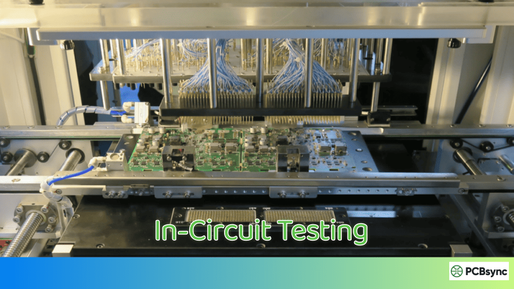
In-circuit testing verifies individual components and circuit paths on a populated PCB. The test system accesses specific test points using pogo pins or probes and measures electrical parameters of each component in isolation.
ICT detects manufacturing defects including:
Defect Type
Detection Method
Solder Shorts
Resistance measurement between adjacent nets
Open Circuits
Continuity verification across expected paths
Wrong Components
Value measurement (R, C, L) comparison
Missing Components
Absence of expected electrical signature
Reversed Polarity
Diode and electrolytic capacitor checks
Damaged ICs
Basic parametric and vector testing
ICT achieves approximately 98% fault coverage for manufacturing defects. The test typically runs with power off, applying small test signals to verify component presence and values without energizing the full circuit.
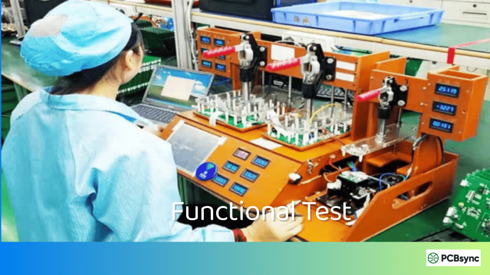
Functional Circuit Testing (FCT) Explained
Functional testing verifies that the assembled PCB operates correctly under real-world conditions. The test system applies power, inputs, and loads to the board and measures outputs against expected specifications.
FCT validates operational characteristics including voltage levels at various nodes, signal timing and frequency response, communication interface functionality, power consumption and efficiency, thermal behavior under load, and response to boundary conditions.
Functional testing catches design issues and marginal components that pass ICT but fail under actual operating conditions. However, when functional tests fail, troubleshooting to root cause can be more challenging because the symptom may not directly indicate the faulty component.
Combining ICT and FCT
Most comprehensive test strategies combine both methods. ICT runs first to catch manufacturing defects quickly and cheaply. Boards passing ICT then proceed to functional testing for operational verification.
Both universal testers and dedicated testers can implement ICT and FCT—the platform choice affects implementation approach rather than capability. Universal systems typically use modular instrumentation to support both methods, while dedicated systems may optimize hardware specifically for one approach.
Test Fixture Design Considerations
Whether you choose universal or dedicated testing, fixture quality dramatically impacts test effectiveness. Poor fixture design creates intermittent failures, slows production, and generates false defects that waste engineering time.
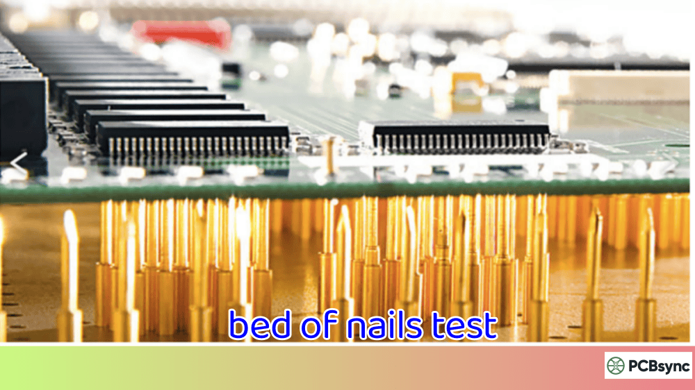
Bed-of-Nails Fixture Fundamentals
The classic bed-of-nails fixture uses spring-loaded pogo pins (also called spring probes) to make temporary electrical contact with test points on the PCB. Key design parameters include:
Pin Selection: Choose pin specifications based on current requirements, contact resistance tolerance, and expected lifecycle. Standard pins handle 2-3A continuous current; high-current applications may require special designs rated for 10A or more.
Pin Pitch: Minimum spacing between adjacent pins affects how many test points you can access. Standard pins accommodate 100-mil (2.54mm) pitch; fine-pitch designs can achieve 50-mil (1.27mm) or tighter with specialty probes.
Contact Force: Each pogo pin exerts force against the PCB—typically 100-200 grams per pin. Multiply by hundreds of pins and you need substantial clamping force. Excessive force risks damaging components or flexing the board.
Alignment Mechanisms: Fixtures must align the PCB precisely to the pin array. Guide pins, edge locators, and optical alignment systems ensure repeatable positioning within thousandths of an inch.
Universal Fixture Architecture
Universal test platforms typically use standardized fixture bases with interchangeable personality modules. The base provides mechanical support, mass interconnect interface, and pneumatic or mechanical actuation. The personality module contains the PCB-specific pogo pin array and routing.
This architecture enables:
Quick fixture swaps (typically under 5 minutes)
Standardized interface to test instrumentation
Reduced fixture storage requirements
Simplified spare parts inventory
The trade-off is some flexibility in fixture design. Personality modules must conform to the base platform’s mechanical and electrical constraints, which may limit optimization for unusual board geometries.
Dedicated Fixture Architecture
Dedicated fixtures can optimize every aspect for the specific PCB. There are no constraints from a universal base platform, allowing engineers to:
Position pins at optimal angles for irregular test point locations
Integrate product-specific handling features (connectors, actuators)
Minimize fixture size for dense production floor layouts
Achieve maximum pin density where needed
The trade-off is higher design cost, longer development time, and limited reusability. When the product design changes significantly, dedicated fixtures often require complete rebuilds rather than modifications.
Flying Probe Testing: The Fixtureless Alternative
Before finalizing your test strategy, consider flying probe testing as a complement to either approach. Flying probe testers use movable probes controlled by software to test PCBs without custom fixtures.
Flying Probe Tester Benefits
Aspect
Flying Probe Advantage
Fixture Cost
Zero ($0 per product)
Setup Time
Hours (program development only)
Design Change Impact
Software update only
Minimum Order Quantity
Economical from 1 piece
Access Capability
Can reach 0.2mm pitch
Flying probe testing costs approximately $500-$2,000 per test program compared to $5,000-$25,000 for traditional fixtures. The trade-off is speed—flying probe tests run sequentially, taking 5-15 minutes per board compared to 15-60 seconds for fixture-based testing.
When Flying Probe Makes Sense
Flying probe testing is ideal for prototypes and pilot builds, low-volume production under 500 units annually, quick-turn manufacturing requirements, and boards with accessibility challenges for traditional fixtures.
Many facilities combine flying probe for low-volume and prototype work with universal or dedicated systems for higher-volume production. This hybrid approach optimizes economics across your entire product portfolio.
Universal Tester Implementation Best Practices
If you decide universal testing fits your operation, these practices will maximize your return on investment:
Platform Selection Criteria
Choose a platform with modular instrumentation that can scale with your needs. Start with core capabilities and add specialized instruments as product requirements demand. Ensure the vendor has a track record of supporting the platform long-term—you don’t want to be stuck with orphaned technology.
Fixture Design Standards
Establish fixture design standards that maximize interchangeability. Standardize on connector types, mounting hardware, and interface dimensions. This discipline pays dividends when you’re maintaining fixtures years later.
Test Program Architecture
Develop test programs using modular, reusable code structures. Create libraries for common measurements that can be called across multiple products. This approach dramatically reduces development time for new product introduction.
Documentation Requirements
Universal test systems require more disciplined documentation because operators must understand which fixtures and programs apply to which products. Invest in clear labeling, configuration management, and operator training materials.
Design for Testability (DFT) Guidelines
Your PCB design directly impacts test equipment requirements and costs. Following DFT principles makes testing more effective regardless of whether you use universal or dedicated systems.
Test Point Placement
Design test points into your PCB layout from the beginning. Waiting until design finalization to consider test access inevitably leads to compromises.
DFT Guideline
Recommendation
Test Point Size
Minimum 35 mil (0.9mm) diameter for reliable contact
Test Point Spacing
Minimum 100 mil (2.54mm) center-to-center standard; 50 mil for dense boards
Component Keep-Out
100 mil clearance around test points for probe access
Via as Test Point
Acceptable if via is not tented and meets size requirements
Both-Side Access
Minimize need for dual-sided probing when possible
Net Accessibility
Every critical net should have at least one test point
Signal Routing Considerations
Test equipment capabilities influence how you should route signals:
High-speed signals benefit from test points placed on transmission lines where impedance can be maintained. Avoid stubs or branches to test points that create reflections.
Analog signals should have test points located to minimize noise coupling from adjacent digital traces. Consider adding filtering capacitors near test points for sensitive measurements.
Power distribution networks need test points at multiple locations to verify voltage levels across the board. Include points near both the power input and critical loads.
Boundary Scan Integration
For boards using FPGAs, CPLDs, or processors with JTAG capability, integrate boundary scan testing into your strategy. JTAG test access requires only four or five pins regardless of device complexity, dramatically reducing fixture requirements.
Boundary scan testing complements both universal and dedicated test approaches by providing access to signals that physical probes cannot reach—particularly for BGA packages where solder joints are hidden beneath the component.
Real-World Implementation: A Case Study Approach
Understanding how other manufacturers have approached universal versus dedicated testing decisions can inform your own analysis.
Contract Manufacturer Scenario
A mid-sized EMS provider testing boards for 15 different customers needed to reduce their test equipment footprint while improving changeover efficiency. Their legacy approach used 23 dedicated test stations scattered across the production floor.
After analysis, they implemented three universal test platforms with standardized fixture bases. Each platform could accommodate any of their customer products with appropriate personality modules.
Results after 18 months:
Floor space reduced by 40%
Average changeover time dropped from 45 minutes to 8 minutes
Calibration costs reduced by 60% (fewer instruments to maintain)
New product introduction time decreased from 6 weeks to 3 weeks
Operator training simplified with single platform to master
The investment payback period was 22 months. Ongoing savings continue to accumulate as new customer products integrate onto the existing platforms without additional capital equipment.
High-Volume OEM Scenario
An automotive electronics manufacturer producing 120,000 units monthly of a single control module chose dedicated testing despite the premium cost. Their analysis showed:
For their high-volume stable product, the dedicated system’s throughput advantage translated directly to lower manufacturing costs. The dedicated tester paid for itself in under 12 months through labor savings alone.
Hybrid Implementation
A medical device company adopted a hybrid strategy matching test approach to product lifecycle stage:
Development/Prototype: Flying probe testing for rapid iteration without fixture costs
Low-Volume Production: Universal test platform supporting products under 5,000 units annually
High-Volume Production: Dedicated systems for products exceeding 20,000 units annually
This tiered approach optimized their overall test economics while maintaining appropriate capabilities at each production stage.
Making the Decision: A Practical Framework
To choose between universal and dedicated testing, work through this decision framework:
Step 1: Inventory Your Product Portfolio
List every PCB design you currently test or plan to test. For each product, note the annual production volume, expected product life cycle, design change frequency, and test complexity requirements.
Step 2: Calculate Economics for Both Scenarios
Model the five-year total cost of ownership for both universal and dedicated approaches. Include capital equipment, fixtures, floor space, maintenance, calibration, and operator training. Don’t forget opportunity costs—what else could you do with the capital or floor space?
Step 3: Evaluate Operational Factors
Beyond pure economics, consider how each approach affects your manufacturing agility, quality systems, and workforce development. Sometimes the right answer isn’t the cheapest answer.
Step 4: Plan for Hybrid Implementation
Most operations benefit from a combination of approaches. You might use universal testing for 80% of products by variety but only 30% by volume, with dedicated systems handling your highest-runners.
Frequently Asked Questions
What is the typical ROI timeline for a universal tester investment?
Universal test platforms typically achieve payback within 18-36 months when replacing multiple dedicated stations or enabling faster new product introduction. The exact timeline depends on your product mix, fixture costs avoided, and floor space value. Companies with high product variety often see faster payback than those with stable portfolios.
Can universal testers achieve the same test coverage as dedicated systems?
In most applications, yes. Modern universal test platforms can achieve 98%+ test coverage comparable to dedicated systems. The key is proper fixture design and test program development. However, some specialized applications requiring unique measurement capabilities may still benefit from dedicated optimization.
How do I handle high-volume products in a universal test environment?
For high-volume products tested on universal platforms, consider maintaining multiple identical fixtures to enable parallel testing across multiple stations or shifts. Some facilities also invest in dedicated systems for their absolute highest-volume products while keeping everything else on universal platforms.
What maintenance requirements should I expect for universal testers?
Universal testers consolidate maintenance onto fewer systems, but those systems require more rigorous attention. Plan for annual calibration of all instruments, quarterly fixture inspection and pogo pin replacement, monthly software updates and backup, and ongoing operator training as products change.
How do universal testers integrate with manufacturing execution systems?
Modern universal test platforms offer robust connectivity options including industry-standard interfaces like OPC-UA, REST APIs, and database connectivity. Test results can flow directly into your MES for traceability, SPC analysis, and yield reporting. Ensure your selected platform supports your existing IT infrastructure.
Useful Resources for PCB Testing
These resources provide additional technical depth for your test engineering team:
Industry Standards
IPC-9252: Requirements for Electrical Testing of Unpopulated Printed Boards
IPC-A-610: Acceptability of Electronic Assemblies
JTAG/IEEE 1149.1: Standard Test Access Port and Boundary-Scan Architecture
Test Equipment Manufacturers
National Instruments (NI): Universal test platform solutions
Teradyne: In-circuit test systems
Keysight Technologies: Test instrumentation and software
SPEA: Flying probe and ICT systems
Seica: Flying probe testers
Software and Programming Resources
NI TestStand: Test management software documentation
IEEE (Institute of Electrical and Electronics Engineers)
Conclusion
The choice between universal testers and dedicated testers isn’t about which technology is superior—it’s about matching your test strategy to your manufacturing reality. Universal testing provides the flexibility that modern product portfolios demand, while dedicated testing delivers the throughput that high-volume production requires.
Most successful test operations combine both approaches strategically. They use universal platforms for product variety and development support, then transition high-volume stable products to dedicated systems when economics justify the investment.
Take the time to analyze your specific situation thoroughly. Map your product portfolio, model the economics honestly, and consider both current needs and future direction. The right test strategy provides quality assurance your customers expect while supporting the manufacturing efficiency your business requires.
What works for your operation depends on factors only you can evaluate. But with the framework and information in this guide, you’re equipped to make that decision with confidence.
Inquire: Call 0086-755-23203480, or reach out via the form below/your sales contact to discuss our design, manufacturing, and assembly capabilities.
Quote: Email your PCB files to Sales@pcbsync.com (Preferred for large files) or submit online. We will contact you promptly. Please ensure your email is correct.
Notes: For PCB fabrication, we require PCB design file in Gerber RS-274X format (most preferred), *.PCB/DDB (Protel, inform your program version) format or *.BRD (Eagle) format. For PCB assembly, we require PCB design file in above mentioned format, drilling file and BOM. Click to download BOM template To avoid file missing, please include all files into one folder and compress it into .zip or .rar format.


