Inquire: Call 0086-755-23203480, or reach out via the form below/your sales contact to discuss our design, manufacturing, and assembly capabilities.
Quote: Email your PCB files to Sales@pcbsync.com (Preferred for large files) or submit online. We will contact you promptly. Please ensure your email is correct.
Notes: For PCB fabrication, we require PCB design file in Gerber RS-274X format (most preferred), *.PCB/DDB (Protel, inform your program version) format or *.BRD (Eagle) format. For PCB assembly, we require PCB design file in above mentioned format, drilling file and BOM. Click to download BOM template To avoid file missing, please include all files into one folder and compress it into .zip or .rar format.
How to Generate Gerber Files in Eagle: A Complete Guide for PCB Engineers
Generating Gerber files in Eagle is an essential skill every PCB engineer must master before sending designs to fabrication. Gerber files serve as the universal language between your CAD software and PCB manufacturers, containing all the critical layer information needed to produce your board accurately. This comprehensive guide walks you through the complete workflow for exporting production-ready Gerber files from Autodesk Eagle.
Understanding Gerber Files and Their Importance
Gerber files follow the RS-274X format, an industry-standard specification that describes each layer of your PCB as a series of vector graphics. Unlike native Eagle .brd files, Gerber files are manufacturer-agnostic and contain unambiguous fabrication data. Every copper layer, solder mask, silkscreen, and drill file gets exported as a separate Gerber file, allowing fabrication houses to process each manufacturing step independently.
PCB manufacturers cannot directly interpret Eagle’s proprietary file format. Therefore, converting your design to Gerber format eliminates potential compatibility issues and ensures dimensional accuracy throughout the fabrication process. Modern PCB fabs expect Gerber files as the primary deliverable, making this conversion a non-negotiable step in your design-to-manufacturing pipeline.
Prerequisites Before Gerber Export
Before initiating the export process, verify your design passes all Design Rule Checks (DRC) in Eagle. Any unresolved errors will propagate into your Gerber output and potentially cause manufacturing defects. Additionally, confirm your silkscreen placement—Eagle generates only top-side silkscreen layers (tPlace and tNames) by default. Double-sided silkscreen designs require manual configuration to include bottom layers (bPlace and bNames).
Furthermore, review your board outline on the Dimension layer. Any milling operations or cutouts must be properly defined before export. Taking these preparatory steps prevents costly respins and manufacturing delays downstream.
Step 1: Configuring Drill Files
The drill file configuration establishes the foundation for accurate via and through-hole positioning. Eagle requires you to run a User Language Program (ULP) to generate proper drill configurations before Gerber export.
Navigate to File → Run ULP in your board layout window. In the file browser, locate and select drillcfg.ulp. Eagle presents the Drill Configuration dialog where you can verify tool settings and coordinate formats. Click OK to generate the drill configuration file, which Eagle saves alongside your board file.
This step creates the necessary mapping between your design’s drill definitions and the Excellon format that CNC drilling machines expect. Skipping this configuration often results in incorrect hole sizes or misaligned drill hits during manufacturing.
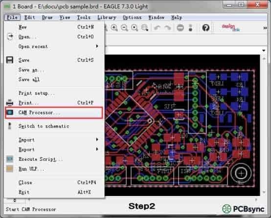
Step 2: Launching the CAM Processor
Eagle’s CAM (Computer-Aided Manufacturing) Processor handles all Gerber generation tasks. Access it by opening your .brd file and selecting File → CAM Processor from the menu bar. The CAM Processor interface displays tabs for each output layer along with format and device settings.
Within the CAM Processor, navigate to File → Open → Job to load a predefined CAM job file. For drill files, select excellon.cam from the available options. This job file contains preconfigured settings optimized for Excellon drill output format, which is universally accepted by PCB manufacturers.
After loading the job, click Process Job to execute the export. Eagle generates the drill file with a .drd extension in your project directory. The accompanying .dri file contains drill station metadata but is typically not required for manufacturing submission.
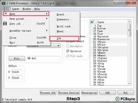
Step 3: Generating Gerber Layer Files
Return to the CAM Processor and load the gerb274x.cam job file using the same File → Open → Job workflow. This job file configures Eagle to output Gerber files in the RS-274X extended format, which includes embedded aperture definitions and eliminates the need for separate aperture files.
The default gerb274x.cam job includes tabs for copper layers, solder mask layers, and top silkscreen. Execute the job by clicking Process Job, and Eagle exports the corresponding Gerber files to your project folder.
However, the default configuration may not capture all required layers for your specific design. Two common scenarios require manual CAM Processor modifications: double-sided silkscreen and milling operations.
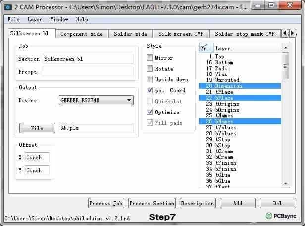
Adding Bottom Silkscreen Layers
For boards with component designators or graphics on both sides, you must manually add a bottom silkscreen section to the CAM job. Click Add in the CAM Processor to create a new output section. Configure the new section with the following parameters:
Set the Section name to “Silkscreen_Bottom” or a similar descriptive identifier. Change the output filename to %N.pls to maintain consistent naming conventions. Deselect all layers, then enable only layers 20 (Dimension), 22 (bPlace), and 26 (bNames). This configuration captures the board outline along with bottom-side placement graphics and component names.
Including Milling and Cutout Data
Internal cutouts, slots, and edge routing require explicit layer configuration in Eagle. Create another CAM section by clicking Add and naming it “Board_Outline” or “Edge_Cuts”. Set the output filename to %N.gko to indicate outline/milling data. Enable layer 20 (Dimension) and layer 46 (Milling) while deselecting all other layers.
This separation ensures manufacturers can distinguish between the board perimeter and internal routing operations. Combining these operations on a single layer often causes interpretation errors during CAM processing at the fab house.
Step 4: Verifying Output Files
After CAM processing completes, your project directory contains multiple output files representing each PCB layer. A standard two-layer board generates the following essential files:
The .cmp file contains top copper layer data, while .sol represents the bottom copper layer. Solder mask files appear as .stc (top) and .sts (bottom), controlling where mask material gets applied during fabrication. Silkscreen layers export as .plc (top) and .pls (bottom) for legend and component marking. The .drd file provides Excellon drill data for all through-holes and vias.
Before submitting to manufacturing, always verify your Gerber output using a standalone Gerber viewer. This independent verification catches layer misalignment, missing features, and aperture issues that might not be apparent in Eagle’s native view. Several free tools exist for this purpose, including online viewers provided by most PCB manufacturers.
Step 5: Packaging for Fabrication
Compress all generated files into a single ZIP archive for submission. Include only the essential manufacturing files—exclude informational outputs like .gpi (photoplotter info) and .dri (drill station info) unless specifically requested by your manufacturer.
Your final package should contain copper layers, solder masks, silkscreen layers, drill files, and board outline data. Most online quoting systems automatically parse these files and display layer previews for confirmation before order placement.
Version-Specific Considerations
Eagle version 9.2.0 and later introduced changes to the default CAM job structure and layer naming conventions. If you experience export issues with newer Eagle releases, consult Autodesk’s updated documentation or use manufacturer-provided CAM job files optimized for your specific Eagle version.
Many fabrication houses offer downloadable CAM job files preconfigured for their manufacturing requirements. Using these vendor-specific jobs ensures layer naming and format compliance while reducing the likelihood of engineering queries during order processing.
Conclusion
Generating Gerber files in Eagle requires systematic attention to drill configuration, layer selection, and output verification. By following this structured workflow—from drill setup through CAM processing to final verification—you ensure your PCB designs translate accurately into manufactured boards. Master this process once, and it becomes a reliable checkpoint in every project, eliminating manufacturing uncertainty and accelerating your path from design to production.
Inquire: Call 0086-755-23203480, or reach out via the form below/your sales contact to discuss our design, manufacturing, and assembly capabilities.
Quote: Email your PCB files to Sales@pcbsync.com (Preferred for large files) or submit online. We will contact you promptly. Please ensure your email is correct.
Notes: For PCB fabrication, we require PCB design file in Gerber RS-274X format (most preferred), *.PCB/DDB (Protel, inform your program version) format or *.BRD (Eagle) format. For PCB assembly, we require PCB design file in above mentioned format, drilling file and BOM. Click to download BOM template To avoid file missing, please include all files into one folder and compress it into .zip or .rar format.


