Inquire: Call 0086-755-23203480, or reach out via the form below/your sales contact to discuss our design, manufacturing, and assembly capabilities.
Quote: Email your PCB files to Sales@pcbsync.com (Preferred for large files) or submit online. We will contact you promptly. Please ensure your email is correct.
Notes: For PCB fabrication, we require PCB design file in Gerber RS-274X format (most preferred), *.PCB/DDB (Protel, inform your program version) format or *.BRD (Eagle) format. For PCB assembly, we require PCB design file in above mentioned format, drilling file and BOM. Click to download BOM template To avoid file missing, please include all files into one folder and compress it into .zip or .rar format.
How to Generate Gerber Files from Altium Designer (DXP): A Complete Engineering Guide
Every PCB design must ultimately be translated into a language that fabrication houses understand—and that language is Gerber. As an industry-standard format, Gerber files contain the precise photolithographic data required to manufacture your printed circuit boards. Altium Designer (DXP) provides robust tools for generating these files, but proper configuration is essential to avoid costly fabrication errors. This guide walks you through the complete process of exporting production-ready Gerber and NC drill files from Altium Designer.
Understanding Gerber Files and Their Role in PCB Manufacturing
Gerber files represent the de facto standard for PCB fabrication data exchange. Originally developed by Gerber Scientific, this vector image format describes each layer of your PCB design—copper layers, solder mask, silkscreen, and paste layers—as discrete files that CAM (Computer-Aided Manufacturing) software can interpret.
When you submit a design to a PCB manufacturer, the fabrication team uses these files to create phototools for each layer. Any misconfiguration in your Gerber output can result in misaligned layers, incorrect apertures, or missing features that compromise the final product. Altium Designer streamlines this process through its integrated output job configuration, but engineers must understand the underlying parameters to ensure manufacturing success.
Prerequisites Before Generating Gerber Output
Before initiating the Gerber export process, verify that your PCB design meets the following criteria:
Your design rule check (DRC) should report zero errors. Unresolved DRC violations may produce Gerber files that fail CAM review or result in manufacturing defects. Additionally, confirm that all layer pairs are correctly defined, particularly for multi-layer boards where inner layer assignments affect drill file generation.
Ensure your board outline is properly defined on the mechanical layer or board outline layer, as manufacturers rely on this boundary for panel creation and routing operations. Finally, verify that your design includes appropriate clearances for manufacturing tolerances—most fabricators require minimum 6-mil trace/space for standard processes.
Step-by-Step: Generating Gerber Files in Altium Designer
The Gerber generation process in Altium Designer involves configuring the output settings, selecting appropriate layers, and defining advanced parameters that match your manufacturer’s requirements.
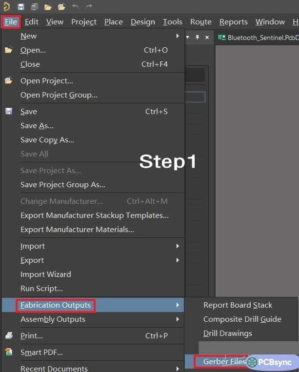
Accessing the Gerber Setup Interface
Navigate to the menu bar and select File → Fabrication Outputs → Gerber Files. This action opens the Gerber Setup dialog, which serves as the central configuration panel for all Gerber output parameters.
The dialog presents multiple tabs for configuring different aspects of the output. Understanding each tab’s function is critical for producing manufacturer-compliant files.
Configuring the Layers to Plot
Within the Gerber Setup interface, locate the Layers to plot page. This section determines which design layers will be exported as individual Gerber files.
Click Plot Layers → Select Used to automatically include all layers containing design data. This option intelligently identifies layers with actual content, eliminating empty layers from the output. For most designs, this automated selection provides comprehensive coverage.
However, certain applications may require manual layer selection. High-density interconnect (HDI) designs or boards with buried/blind vias may need explicit layer configuration to ensure proper via definition across layer pairs.
The standard layer set typically includes:
Top and bottom copper layers
Internal signal and plane layers
Top and bottom solder mask
Top and bottom silkscreen (overlay)
Top and bottom paste layers
Mechanical layers for board outline
Advanced Gerber Settings Configuration
Select the Advanced tab to access parameters that directly affect file compatibility and precision. These settings require careful consideration based on your fabricator’s specifications.
Format Configuration: Most modern fabricators accept RS-274X extended Gerber format, which embeds aperture definitions within the file itself. This format eliminates the need for separate aperture lists and reduces the risk of aperture assignment errors during CAM processing.
Precision Settings: Configure the coordinate precision to match your design requirements. For designs with fine-pitch components or tight tolerances, higher precision (2:5 or 2:6 format for metric units) ensures accurate feature placement. The 2:5 format provides 0.00001mm resolution, suitable for most applications.
Units Selection: Select units consistent with your design database. Mixing imperial and metric units between design and output can introduce conversion errors, particularly for pad dimensions and trace widths.
After configuring all parameters, click Apply to generate the Gerber files. Altium Designer will create a CAM project file (.Cam) containing the output. You may close this project file without saving—the actual Gerber files have already been written to your designated output directory.
Generating NC Drill Files for Hole Data
Gerber files alone do not contain drilling information. NC (Numerical Control) drill files must be generated separately to communicate hole locations, sizes, and plating requirements to the fabricator’s drilling equipment.
Accessing NC Drill Setup
From the menu bar, select File → Fabrication Outputs → NC Drill Files. This opens the NC Drill Setup dialog, where you configure drilling parameters and format specifications.
Configuring Drill Output Parameters
Within the NC Drill Setup interface, configure the following critical parameters:
Units: Select inches or millimeters consistent with your Gerber output and manufacturer preferences. Most fabricators accept either format but specify a preference in their design guidelines.
Format: The 2:5 format provides appropriate precision for most designs, offering 0.00001-inch resolution for imperial units. High-precision applications may require 2:6 format.
Zero Suppression: Configure leading or trailing zero suppression based on your manufacturer’s requirements. Trailing zero suppression (TZ) is common, but verify this specification with your fabricator to prevent coordinate interpretation errors.
Click OK to generate the drill files. An Import Drill Data dialog may appear—maintain default settings and click OK to proceed. The system generates the NC drill output, which you can close without saving the temporary CAM project.
Verifying Your Output Files
After generation, your project directory contains the complete fabrication dataset. A typical output includes:
Individual Gerber files for each layer (extensions vary by layer type)
NC drill file(s) with hole location data
Optional aperture and tool reports
Before submitting files to your manufacturer, perform verification using a standalone Gerber viewer. Many free tools exist for this purpose, including Altium’s built-in CAMtastic viewer, GerbView, or online viewers provided by fabricators. Verification should confirm layer alignment, feature completeness, and drill-to-copper registration.
Common Configuration Issues and Solutions
Engineers frequently encounter several issues during Gerber generation that warrant attention.
Missing Layers: If certain layers appear absent from output, verify layer visibility settings and confirm that design data exists on those layers. Empty layers are automatically excluded when using “Select Used” option.
Aperture Errors: RS-274X format typically prevents aperture issues, but legacy RS-274D format requires manual aperture assignment. Always prefer extended Gerber format unless specifically required otherwise.
Coordinate Offset: If designs appear shifted in the viewer, check the origin settings in your PCB design. Manufacturers prefer designs positioned at positive coordinates relative to the origin.
Drill-to-Copper Misalignment: This typically indicates unit mismatch between Gerber and drill files. Ensure consistent unit selection across all output configurations.
Best Practices for Production-Ready Output
Implementing these practices ensures smooth fabrication processing:
Generate all fabrication files simultaneously from a verified design to maintain consistency. Include a fabrication drawing or README specifying layer stackup, material requirements, and special instructions. Compress all output files into a single archive for submission, reducing the risk of missing files.
Maintain version control for your output configurations, particularly for designs requiring frequent revision. Altium Designer’s Output Job files (.OutJob) enable standardized, repeatable output generation across design iterations.
Conclusion
Generating accurate Gerber files from Altium Designer requires understanding both the software interface and manufacturing requirements. By properly configuring layer selection, format parameters, and drill output settings, engineers can produce fabrication-ready files that minimize CAM processing issues and manufacturing delays. Always verify output files before submission and maintain clear communication with your fabrication partner regarding any special requirements or specifications.
The process outlined here—accessing Gerber setup, selecting used layers, configuring advanced settings, and generating companion drill files—provides a reliable workflow for any PCB complexity level. Master these fundamentals, and your designs will transition smoothly from digital concept to physical reality.
Inquire: Call 0086-755-23203480, or reach out via the form below/your sales contact to discuss our design, manufacturing, and assembly capabilities.
Quote: Email your PCB files to Sales@pcbsync.com (Preferred for large files) or submit online. We will contact you promptly. Please ensure your email is correct.
Notes: For PCB fabrication, we require PCB design file in Gerber RS-274X format (most preferred), *.PCB/DDB (Protel, inform your program version) format or *.BRD (Eagle) format. For PCB assembly, we require PCB design file in above mentioned format, drilling file and BOM. Click to download BOM template To avoid file missing, please include all files into one folder and compress it into .zip or .rar format.


