Inquire: Call 0086-755-23203480, or reach out via the form below/your sales contact to discuss our design, manufacturing, and assembly capabilities.
Quote: Email your PCB files to Sales@pcbsync.com (Preferred for large files) or submit online. We will contact you promptly. Please ensure your email is correct.
Notes: For PCB fabrication, we require PCB design file in Gerber RS-274X format (most preferred), *.PCB/DDB (Protel, inform your program version) format or *.BRD (Eagle) format. For PCB assembly, we require PCB design file in above mentioned format, drilling file and BOM. Click to download BOM template To avoid file missing, please include all files into one folder and compress it into .zip or .rar format.
How to Generate Gerber and Drill Files in KiCad 8.0
Generating Gerber and drill files in KiCad 8.0 represents the critical bridge between your PCB design and physical fabrication. These manufacturing files communicate your design intent to PCB fabricators with precision, defining every copper trace, drill hole, and soldermask opening. This comprehensive guide walks you through the complete export workflow with production-proven settings that ensure first-pass manufacturing success.
What Are Gerber and Drill Files?
Gerber files follow the RS-274X standard (or the newer X2 extension) and describe each layer of your PCB as vector graphics. Every copper layer, soldermask layer, silkscreen layer, and board outline gets exported as a separate Gerber file. Manufacturers load these files into their CAM software to generate photomasks and toolpaths for production.
Drill files use the Excellon format to specify hole locations, diameters, and plating requirements. Your fabricator’s CNC drilling machines read these files directly to produce all through-holes, vias, and mounting holes in your design.
Together, these files form a complete manufacturing package. Incorrect settings or missing files result in production delays, engineering queries, or defective boards—outcomes every engineer wants to avoid.
Pre-Export Checklist: Run DRC First
Before generating any fabrication outputs, run a Design Rule Check (DRC) on your layout. KiCad 8.0’s DRC engine catches clearance violations, unconnected nets, minimum annular ring violations, and other issues that could cause manufacturing problems or functional failures.
Access DRC through Inspect → Design Rules Checker in the PCB editor. Address all errors before proceeding—warnings also deserve attention since they often indicate borderline manufacturability concerns. A clean DRC report significantly reduces the likelihood of engineering queries from your fabricator.
Step-by-Step Guide to Generate Gerber Files in KiCad 8.0
Open your PCB layout file (.kicad_pcb extension) in KiCad’s PCB editor. Navigate to File → Fabrication Outputs → Gerbers (.gbr)… to launch the Plot dialog window.
Configuring the Output Directory
First, specify your output directory. Best practice dictates creating a dedicated subfolder within your project directory—commonly named “gerber,” “CAM,” or “fabrication.” This organizational approach keeps manufacturing files separate from design files and simplifies archive management.
Selecting Layers for Export
The Plot dialog displays all available layers with checkboxes. For a standard two-layer board, select these layers:
Copper layers: F.Cu (front copper) and B.Cu (back copper) define your signal routing and power distribution.
Soldermask layers: F.Mask and B.Mask specify where soldermask should NOT appear, exposing pads for soldering.
Silkscreen layers: F.Silkscreen and B.Silkscreen contain reference designators, component outlines, and assembly markings.
Paste layers: F.Paste and B.Paste define stencil apertures for solder paste application during SMT assembly.
Board outline: Edge.Cuts defines your board’s physical boundary and any internal cutouts.
For multilayer designs, include all internal copper layers (In1.Cu, In2.Cu, etc.) corresponding to your stackup configuration.
Configuring Plot Settings
The General Options section controls critical export parameters:
Plot format: Select Gerber. KiCad 8.0 defaults to the X2 format with extended attributes, which most modern fabricators accept. If your manufacturer requires legacy RS-274X format, disable “Use Gerber X2 format” and “Include Gerber attributes.”
Coordinate format: Use 4.6 format, providing four integer digits and six decimal places. This delivers 0.001 mil resolution—far exceeding practical manufacturing tolerances while maintaining universal compatibility.
Use drill/place file origin: Enable this option to maintain consistent coordinate references between Gerber files and drill files. Misaligned origins cause registration problems during fabrication.
Essential Gerber Options
Enable these checkboxes for production-ready output:
Check zone fills before plotting: This option verifies that all copper pours are current. If zone fills have become stale due to design changes, KiCad prompts you to refill them before export. Always accept this prompt—outdated zones cause copper discrepancies between your design database and manufactured board.
Subtract soldermask from silkscreen: Prevents silkscreen ink from printing over exposed pads, which would interfere with soldering.
Plot footprint values and Plot reference designators: Include these for documentation purposes, though you may disable them for layers where they’re unnecessary.
Executing the Plot
Click the Plot button to generate your Gerber files. KiCad creates one file per selected layer, automatically applying industry-standard extensions. Monitor the message panel for any warnings or errors during generation.
Step-by-Step Guide to Generate Drill Files in KiCad 8.0
From the same Plot dialog, click Generate Drill Files… in the lower-right corner. This opens the dedicated drill file configuration window.
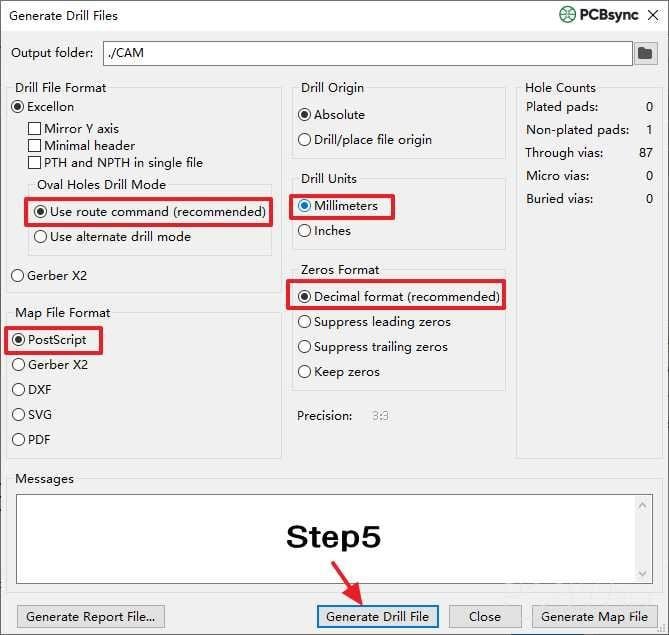
Drill File Format Configuration
Configure these settings for manufacturing compatibility:
Drill file format: Select Excellon. This industry-standard format enjoys universal support across PCB fabricators worldwide.
Drill units: Choose millimeters for metric designs or inches for imperial designs. Match your design units for consistency and easier verification.
Zeros format: Select “Decimal format” for modern CNC equipment. This format offers the clearest representation and works with virtually all contemporary drilling machines.
Drill Origin Settings
Set your drill origin to match the Gerber file origin—use “Drill/place file origin” if you enabled the corresponding option during Gerber generation. Origin consistency between Gerber and drill files is absolutely critical; misaligned origins cause registration errors that can render boards unusable.
Map File Options
Select a map file format (Gerber X2, PostScript, or PDF) for visual verification. The drill map provides a graphical representation of all hole locations and sizes, useful for quick sanity checks before submission.
PTH and NPTH Handling
KiCad generates separate files for Plated Through-Holes (PTH) and Non-Plated Through-Holes (NPTH) by default. Most fabricators handle this automatically, but some prefer combined files. Check your manufacturer’s requirements if uncertain.
For designs with blind or buried vias, KiCad automatically generates additional drill files for each via span. Verify these files exist if your design uses HDI structures.
Generating the Output
Click Generate Drill File to create your Excellon files. The output includes drill files and optionally a drill report listing all hole sizes and counts—useful for cost estimation and manufacturability review.
Verifying Your Manufacturing Package
Never submit unverified fabrication files. KiCad 8.0 includes GerbView, a standalone Gerber viewer accessible through the application launcher or via File → Open → Gerber Viewer.
Import all generated files and systematically verify:
Layer alignment: All layers should register correctly to each other. Check pad-to-drill alignment especially carefully.
Copper coverage: Verify that zone fills appear complete and connect properly to their nets.
Board outline: Confirm the Edge.Cuts layer forms a closed contour with no gaps.
Drill accuracy: Overlay drill files on copper layers to verify hole positions align with pad centers.
Many PCB manufacturers offer online Gerber viewers that perform additional DFM (Design for Manufacturability) checks against their specific capabilities. Use these tools for additional verification before placing orders.
Packaging Files for Submission
Compress all Gerber and drill files into a single ZIP archive for submission. Place all files at the archive root level without nested folders—this simplifies automated processing at the fabrication facility.
Include a brief README specifying your stackup, copper weight, surface finish, and any special requirements. While online quoting systems capture most parameters, explicit documentation prevents misunderstandings on complex or unusual orders.
Conclusion
Successfully generating Gerber and drill files in KiCad 8.0 requires attention to detail at every step. Run DRC before export, configure plot settings carefully, maintain origin consistency between Gerber and drill files, and verify everything before submission. This disciplined approach ensures your boards manufacture correctly on the first attempt, saving time, money, and engineering frustration.
The export process itself takes only minutes once you understand the workflow. The verification step takes longer but pays dividends in avoided respins and manufacturing delays. Treat your fabrication output with the same engineering rigor you apply to your design work, and your boards will consistently match your design intent.
Inquire: Call 0086-755-23203480, or reach out via the form below/your sales contact to discuss our design, manufacturing, and assembly capabilities.
Quote: Email your PCB files to Sales@pcbsync.com (Preferred for large files) or submit online. We will contact you promptly. Please ensure your email is correct.
Notes: For PCB fabrication, we require PCB design file in Gerber RS-274X format (most preferred), *.PCB/DDB (Protel, inform your program version) format or *.BRD (Eagle) format. For PCB assembly, we require PCB design file in above mentioned format, drilling file and BOM. Click to download BOM template To avoid file missing, please include all files into one folder and compress it into .zip or .rar format.


