Inquire: Call 0086-755-23203480, or reach out via the form below/your sales contact to discuss our design, manufacturing, and assembly capabilities.
Quote: Email your PCB files to Sales@pcbsync.com (Preferred for large files) or submit online. We will contact you promptly. Please ensure your email is correct.
Notes: For PCB fabrication, we require PCB design file in Gerber RS-274X format (most preferred), *.PCB/DDB (Protel, inform your program version) format or *.BRD (Eagle) format. For PCB assembly, we require PCB design file in above mentioned format, drilling file and BOM. Click to download BOM template To avoid file missing, please include all files into one folder and compress it into .zip or .rar format.
How to Generate Gerber and Drill Files From Eagle 9.6.2
Generating Gerber and drill files from Eagle 9.6.2 is an essential step in transitioning your PCB design from the digital environment to physical fabrication. Gerber files serve as the industry-standard format that PCB manufacturers use to produce your boards, containing all the layer-specific information needed for accurate fabrication. This comprehensive guide walks you through the complete workflow for exporting production-ready files from Autodesk Eagle 9.6.2.
Understanding Gerber Files and Their Importance in PCB Manufacturing
Before diving into the export process, it’s crucial to understand what Gerber files actually represent. The Gerber format (RS-274X) is a vector image format that describes each layer of your PCB design separately. A complete Gerber package typically includes copper layers, solder mask layers, silkscreen layers, paste layers, and board outline definitions. Additionally, drill files (Excellon format) specify the precise locations and diameters of all holes on your board.
PCB fabrication houses worldwide accept Gerber files as their primary input format because of their standardized nature and precision. Unlike native design files (such as Eagle’s .brd format), Gerber files provide an unambiguous representation of your design that eliminates potential interpretation errors during manufacturing. Therefore, mastering the Gerber export process is fundamental for any hardware engineer working with Eagle.
Prerequisites and Pre-Export Verification
Before exporting your Gerber files, several preparatory steps will help ensure a smooth manufacturing process. First, always run a comprehensive Design Rule Check (DRC) on your board. Eagle’s DRC functionality validates your design against manufacturer specifications, catching potential issues like insufficient trace clearances, drill size violations, or unconnected nets.
To access DRC in Eagle 9.6.2, navigate to Tools > DRC or click the DRC icon in the toolbar. Configure the rules according to your fabrication house’s capabilities—most manufacturers provide downloadable DRC files tailored to their processes. Resolving all DRC errors before Gerber export prevents costly respins and manufacturing delays.
Furthermore, verify that your design layers are properly configured. Eagle uses a layer-based system where different design elements reside on specific layers. Confirm that your copper pours are correctly assigned, your silkscreen doesn’t overlap solder pads, and your board outline is clearly defined on the appropriate layer (typically layer 20, Dimension).
Step-by-Step Gerber Export Process in Eagle 9.6.2
The Gerber generation workflow in Eagle 9.6.2 utilizes the CAM Processor, a powerful tool that converts your design data into manufacturing-ready formats. Follow these steps to export your files correctly.
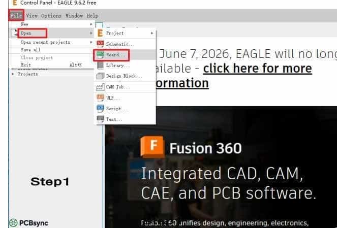
Opening Your Design File
Launch Eagle’s Control Panel and navigate to File > Open > Board. Select the .brd file you wish to export. Your PCB layout will appear in the main editor window, displaying all design elements across their respective layers. Take a moment to visually inspect your design for any obvious issues before proceeding.
Accessing the CAM Processor
Locate the CAM Processor button in the toolbar—it’s the icon without the green arrow. Alternatively, access it through File > CAM Processor. The CAM Processor window presents options for configuring your output files, including layer selections, file formats, and export parameters.
Loading the Appropriate CAM Job
Eagle includes pre-configured CAM jobs that simplify the export process for common board configurations. Click the document icon adjacent to the CAM file name field, then navigate to Load CAM Jobs > examples. Select the job file matching your board’s layer count. For a standard two-layer design, choose “example_2_layer.cam”—this template automatically configures the correct layer mappings for top copper, bottom copper, solder masks, silkscreen, and drill files.
Once your CAM job loads, the interface displays tabs representing each output file. Use the Gerber previewer on the right side to inspect individual layers visually. This preview functionality allows you to verify that each layer contains the expected design elements before committing to export.
Pay particular attention to the “Negative image” checkbox—this option should remain unchecked for most standard exports. Enabling negative mode inverts the layer output, which causes manufacturing errors unless your fabrication process specifically requires inverted data.
Generating the Output Package
Enable the “Export as ZIP” option to consolidate all Gerber and drill files into a single compressed archive. This packaging approach simplifies file handling when uploading to your manufacturer’s ordering portal. Click “Process Job” to execute the export operation.
Eagle generates the ZIP file in your project directory. The archive contains individual Gerber files for each layer (.GTL for top copper, .GBL for bottom copper, .GTS for top solder mask, .GBS for bottom solder mask, .GTO for top silkscreen, .GBO for bottom silkscreen) along with drill files (.DRL or .XLN extension) and any additional layers your CAM job specified.
Verifying Your Gerber Output
Post-export verification is a critical quality assurance step that many engineers unfortunately skip. Before submitting files to manufacturing, inspect your Gerbers using a dedicated viewer application. Several free options exist, including online tools that allow drag-and-drop file inspection without software installation.
When reviewing your Gerber files, check for proper layer alignment—copper features should align precisely with drill holes, solder mask openings should correctly expose pads, and silkscreen text should remain legible and properly positioned. Look for any unexpected artifacts, missing features, or layer registration problems.
Additionally, verify your drill file contains accurate hole specifications. Open the drill file in a text editor to confirm that tool definitions match your design intent. The file header typically lists each drill size alongside its designation code, followed by coordinate data for every hole location.
Common Export Issues and Troubleshooting
Several issues frequently arise during Gerber generation. Layer misalignment typically results from incorrect CAM job configuration—verify that each output tab references the correct source layers. Missing features often indicate that design elements reside on unexpected layers; review your layer assignments in the board editor.
If your manufacturer reports file format incompatibilities, confirm you’re using the RS-274X extended Gerber format rather than the obsolete RS-274D standard. Eagle 9.6.2 defaults to RS-274X, but custom CAM configurations might specify otherwise.
For complex boards with impedance-controlled traces or special requirements, coordinate with your fabrication house regarding any additional documentation they need beyond standard Gerbers—this might include layer stack-up specifications, impedance requirements, or special processing instructions.
Conclusion
Generating accurate Gerber and drill files from Eagle 9.6.2 requires attention to detail throughout the export workflow. By performing pre-export DRC verification, selecting appropriate CAM job templates, and validating your output files before submission, you minimize the risk of manufacturing errors and project delays. The systematic approach outlined in this guide ensures your designs transition smoothly from Eagle’s design environment to physical production, maintaining fidelity to your original engineering intent.
Inquire: Call 0086-755-23203480, or reach out via the form below/your sales contact to discuss our design, manufacturing, and assembly capabilities.
Quote: Email your PCB files to Sales@pcbsync.com (Preferred for large files) or submit online. We will contact you promptly. Please ensure your email is correct.
Notes: For PCB fabrication, we require PCB design file in Gerber RS-274X format (most preferred), *.PCB/DDB (Protel, inform your program version) format or *.BRD (Eagle) format. For PCB assembly, we require PCB design file in above mentioned format, drilling file and BOM. Click to download BOM template To avoid file missing, please include all files into one folder and compress it into .zip or .rar format.


