Inquire: Call 0086-755-23203480, or reach out via the form below/your sales contact to discuss our design, manufacturing, and assembly capabilities.
Quote: Email your PCB files to Sales@pcbsync.com (Preferred for large files) or submit online. We will contact you promptly. Please ensure your email is correct.
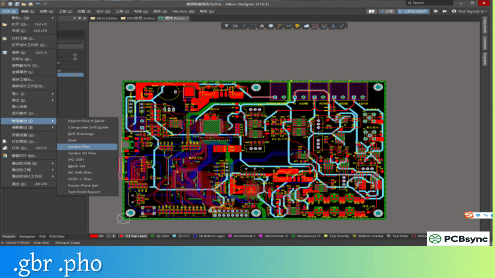
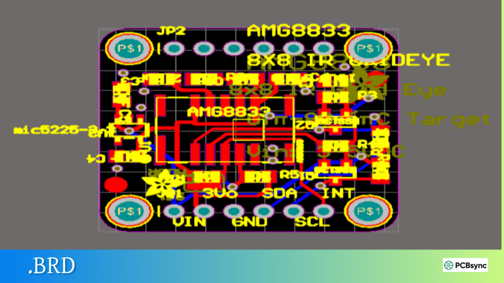
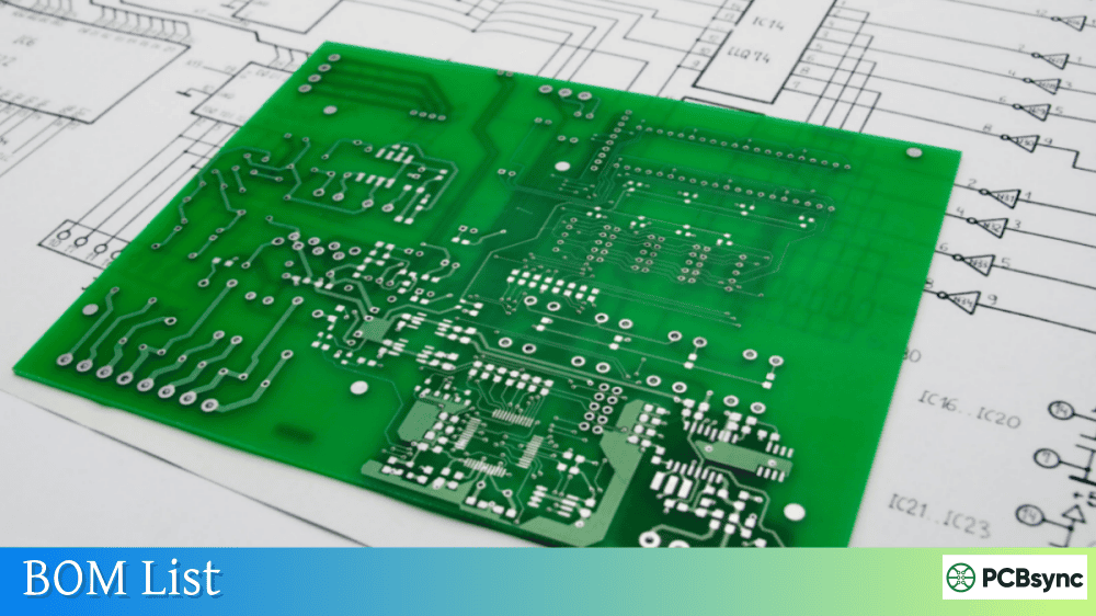
Notes: For PCB fabrication, we require PCB design file in Gerber RS-274X format (most preferred), *.PCB/DDB (Protel, inform your program version) format or *.BRD (Eagle) format. For PCB assembly, we require PCB design file in above mentioned format, drilling file and BOM. Click to download BOM template To avoid file missing, please include all files into one folder and compress it into .zip or .rar format.
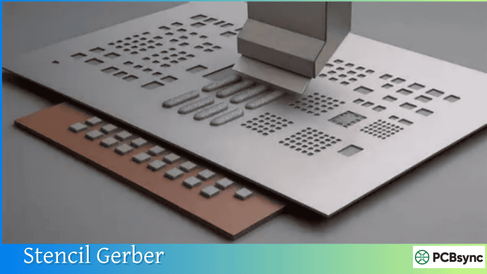
What is a Stencil Gerber File? Complete Solder Paste Stencil Guide
After spending over a decade assembling surface mount boards, I can tell you that the difference between a successful SMT assembly and a nightmare debugging session often comes down to one thing: your stencil Gerber file. Whether you’re building your first prototype or scaling up production, understanding how to properly generate and use stencil Gerber files will save you countless hours of rework.
This guide breaks down everything you need to know about stencil Gerber files, from basic concepts to advanced aperture design considerations that will improve your solder paste deposition.
A stencil Gerber file is a specialized Gerber format file containing the paste layer data from your PCB design. This file defines the aperture locations and sizes that will be laser-cut into a thin sheet of stainless steel or polyimide material to create your solder paste stencil.
When you export your PCB design for manufacturing, the stencil Gerber file represents a “map” of all the surface mount pads where solder paste needs to be applied. The file uses the RS-274X (Extended Gerber) format, which is the industry standard recognized by virtually all stencil manufacturers worldwide.
Stencil Gerber File Extensions Explained
Different PCB design software packages use various naming conventions, but the standard extensions you’ll encounter include:
File Extension
Description
Layer Function
.GTP
Gerber Top Paste
Top side solder paste stencil
.GBP
Gerber Bottom Paste
Bottom side solder paste stencil (mirrored)
.tCream
Top Cream Layer
EAGLE software naming convention
.bCream
Bottom Cream Layer
EAGLE software naming convention
F.Paste
Front Paste
KiCad naming convention
B.Paste
Back Paste
KiCad naming convention
.pmc
Paste Mask Component
Altium Designer convention
.pms
Paste Mask Solder
Altium Designer convention
The key thing to remember is that regardless of the extension, these files all serve the same purpose: defining where solder paste should be deposited on your PCB.
Why Stencil Gerber Files Matter for PCB Assembly
Here’s something that took me years to fully appreciate: according to industry data, 60-70% of all soldering defects originate from issues during the solder paste printing process. Your stencil Gerber file is the foundation of that entire process.
When you lay a stencil over your bare board and squeegee solder paste across it, the apertures in the stencil determine exactly how much paste lands on each pad. Get this wrong, and you’re looking at bridging between fine-pitch pins, tombstoning on small passives, or insufficient solder joints that fail under thermal stress.
Benefits of Using Properly Generated Stencil Gerber Files
The advantages of getting your stencil Gerber files right include:
Improved Assembly Accuracy: Machine placement relies on consistent solder paste volumes. When your stencil Gerber apertures match your actual pad geometry, component self-alignment during reflow works as intended.
Reduced Manufacturing Costs: Proper paste volume means fewer defects, less rework, and faster throughput. I’ve seen shops cut their defect rates by more than half just by optimizing their stencil design.
Shorter Turnaround Time: When you send correctly formatted stencil Gerber files, manufacturers can cut your stencil without back-and-forth clarifications. That means faster delivery and quicker assembly cycles.
Better Solder Joint Reliability: The right paste volume produces joints that meet IPC-A-610 workmanship standards. Too little paste creates weak joints; too much causes shorts and solder balls.
How to Generate Stencil Gerber Files
The process varies depending on your PCB design software, but the fundamental concept remains the same: you need to export only the paste layers in Gerber RS-274X format.
Generating Stencil Gerber Files in Autodesk EAGLE
If you’re using EAGLE, follow these steps:
Open your PCB layout file (.brd)
Click the CAM Processor icon in the top toolbar
Deselect all default layers in the CAM Processor dialog
Select Layer 31 (tCream) for the top stencil
Set the Device dropdown to “Gerber_RS274X”
Name your output file (e.g., stencil_top.gtp)
Click “Process Job” to generate the file
Repeat with Layer 32 (bCream) for bottom side if needed
Pro tip: Always include Layer 20 (Dimension) with your paste layer. This gives the stencil manufacturer a reference for board alignment and helps with registration.
Generating Stencil Gerber Files in KiCad
For KiCad users:
Open your PCB in Pcbnew
Go to File → Plot
In the Plot Format dropdown, select “Gerber”
Under included layers, select “F.Paste” (front paste) and “B.Paste” (back paste)
Enable “Use Protel filename extensions” if your manufacturer prefers .GTP/.GBP naming
Click Plot to generate your files
Generating Stencil Gerber Files in Altium Designer
Altium users should:
Open the PCB document
Navigate to File → Fabrication Outputs → Gerber Files
In the Gerber Setup dialog, add the “Paste Mask Top” and “Paste Mask Bottom” layers
Configure your output settings (RS-274X format, appropriate units)
Generate the outputs
Understanding Stencil Gerber Aperture Design
This is where things get interesting from an engineering perspective. The apertures in your stencil aren’t just holes—they’re precision-engineered features that control paste volume and release characteristics.
Critical Aperture Ratios for Stencil Gerber Design
Two ratios govern whether solder paste will release cleanly from your stencil:
Ratio Type
Formula
Minimum Value
Purpose
Aspect Ratio
Aperture Width ÷ Stencil Thickness
≥ 1.5
Ensures paste releases from aperture walls
Area Ratio
Aperture Area ÷ Wall Surface Area
≥ 0.66
Predicts overall paste release efficiency
For a rectangular aperture, the Area Ratio is calculated as: Area Ratio = (L × W) ÷ [2 × (L + W) × T]
Where L = length, W = width, and T = stencil thickness.
When either ratio falls below the threshold, solder paste tends to stick to the aperture walls due to surface tension, resulting in insufficient paste on the pad.
Stencil Thickness Selection Guidelines
Choosing the right stencil thickness is a balancing act. Here’s what I’ve found works in practice:
Component Type
Pitch
Recommended Stencil Thickness
Standard SMD (0805, 0603)
N/A
0.15mm (6 mil)
Fine-pitch QFP
0.5mm
0.12-0.13mm (5 mil)
Ultra fine-pitch QFP/QFN
≤0.4mm
0.10mm (4 mil)
BGA (standard)
>1.0mm
0.15mm (6 mil)
BGA (fine-pitch)
0.5-1.0mm
0.12-0.13mm (5 mil)
Large connectors/thermal pads
N/A
0.15-0.20mm (6-8 mil)
If your board has both fine-pitch ICs and large components, consider a stepped stencil. These have varying thicknesses across different areas, allowing you to deposit less paste on fine-pitch pads while maintaining adequate volume for larger components.
Stencil Gerber File Best Practices
After troubleshooting hundreds of assembly issues, I’ve developed a checklist that I run through before sending any stencil Gerber files to manufacturing.
Aperture Size Modifications
Most stencil Gerber files shouldn’t use a direct 1:1 copy of your pad geometries. Here’s why:
Standard Reduction: For most SMD pads, reduce aperture dimensions by about 2 mil (0.05mm) per side. This creates a slight “gasket” effect that prevents paste from squeezing under the stencil during printing.
Fine-Pitch Components: For pitches below 0.5mm, consider reducing apertures to 85% of pad width while extending length to 110% of pad length. This compensates for the reduced paste volume while maintaining coverage.
BGA Apertures: For BGAs with pitch greater than 1.0mm, use 1:1 aperture sizing. For finer pitch BGAs, reduce circular apertures by 0.05mm from pad diameter.
QFN Center Pads: Large thermal pads on QFN packages benefit from segmented aperture designs (windows or grids) rather than one large opening. This controls paste volume and reduces voiding under the component.
Fiducial Marks in Stencil Gerber Files
If you’re using automated stencil printers, include fiducial marks in your stencil Gerber design. These alignment features allow the printer to precisely position the stencil relative to the PCB.
Standard fiducial specifications:
Diameter: 1mm circular
Minimum clearance: 3mm from other features
Placement: At least two fiducials on diagonal corners
File Naming and Organization
When preparing your stencil Gerber files for manufacturing, clear naming prevents confusion:
Even experienced engineers run into issues. Here are the most common problems I see:
Problem: Solder Bridging Between Pads
Cause: Apertures too large or stencil too thick for component pitch
Solution: Reduce aperture dimensions by 10-15%, or switch to a thinner stencil. For pitches below 0.5mm, consider electropolished stencils for better paste release.
Problem: Insufficient Solder on Joints
Cause: Apertures too small, low area ratio, or paste sticking in apertures
Solution: Verify your area ratio meets the 0.66 minimum. If the ratio is acceptable but paste still sticks, try a nano-coated stencil or adjust your paste chemistry.
Problem: Solder Balls Around Components
Cause: Excessive paste volume, especially near small chip components
Solution: Use home-plate shaped apertures for small passives like 0402s. This reduces paste at the component termination edges where solder balls typically form.
Problem: Tombstoning on Small Passives
Cause: Uneven paste distribution between pads, often due to aperture misalignment or thermal imbalance
Solution: Ensure apertures are identically sized for both pads. Consider offsetting apertures slightly toward the component body center to balance surface tension during reflow.
Stencil Types and Manufacturing Methods
Understanding how stencils are manufactured helps you specify the right product for your application.
Laser-Cut Stainless Steel Stencils
The industry standard for production work. A high-power laser cuts apertures into 304-grade stainless steel with accuracy down to ±0.003mm. Suitable for thousands of print cycles.
Best for: Production runs, fine-pitch components, high reliability requirements
Electroformed Nickel Stencils
Produced through electrochemical deposition, these stencils have extremely smooth aperture walls. The nickel material naturally releases paste better than steel.
Laser-cut from polyimide film, these are affordable alternatives for prototyping. They’re limited to perhaps 10-100 prints before wearing out.
Best for: Prototyping, low-volume work, cost-sensitive projects
Surface Treatments for Stencil Gerber Manufacturing
Treatment
Description
Use Case
Electropolishing
Smooths aperture walls by removing micro-burrs
Fine-pitch ICs (≤0.5mm pitch)
Nano-coating
Hydrophobic polymer layer for improved paste release
BGA, QFN, high-volume production
Step-up
Localized thicker areas
Pin-in-paste, large thermal pads
Step-down
Localized thinner areas
Mixed component boards with fine-pitch
Useful Resources for Stencil Gerber File Creation
Here are tools and suppliers I’ve found reliable over the years:
Gerber Viewing and Editing Software
Software
Cost
Platform
Link
Gerbv
Free
Windows/Linux
gerbv.sourceforge.net
ViewMate
Free
Windows
pentalogix.com
KiCad Gerber Viewer
Free
Cross-platform
kicad.org
Ucamco Reference Viewer
Free
Web-based
gerber-viewer.ucamco.com
CAM350
Commercial
Windows
downstream.com
Stencil Suppliers and Services
Supplier
Specialty
Starting Price
OSH Stencils
Prototyping, Kapton & Steel
~$5
JLCPCB
Production, Nano-coating
~$2-5
PCBWay
Custom sizes, Electropolishing
~$5-10
Stencils Unlimited
High-precision, Electroformed
Contact for quote
Photo Stencil
Production, Quick-turn
Contact for quote
Industry Standards and Documentation
IPC-7525: Stencil Design Guidelines
IPC-7351: Generic Requirements for Surface Mount Design and Land Pattern Standard
IPC-A-610: Acceptability of Electronic Assemblies
Frequently Asked Questions About Stencil Gerber Files
What file format should I use for my stencil Gerber?
Always use RS-274X (Extended Gerber) format. This is the modern standard that includes aperture definitions within the file itself. Avoid the obsolete RS-274D format, which requires separate aperture definition files and is prone to interpretation errors.
Can I use the same stencil Gerber file for both framed and frameless stencils?
Yes, the stencil Gerber file itself doesn’t change based on the stencil frame type. The frame is a manufacturing choice that affects how the stencil mounts in your printing equipment. Frameless stencils work well for hand assembly and small runs, while framed stencils are necessary for automated stencil printers.
How do I modify apertures in my stencil Gerber file without changing my PCB design?
You have two options. First, you can edit the paste layer directly in your PCB software before exporting—most tools allow you to set paste expansion or contraction parameters per pad or globally. Second, you can use Gerber editing software like ViewMate or CAM350 to modify apertures after export. The “swell” function lets you increase or decrease aperture dimensions across the entire file.
Should I include my board outline in the stencil Gerber file?
Absolutely. Including the board outline (mechanical layer) helps the stencil manufacturer understand the relationship between apertures and board edges. It also enables them to add proper alignment features and choose an appropriate stencil frame size. Some manufacturers even use the outline to create jigs for manual alignment.
What stencil thickness should I specify for a board with mixed component sizes?
For boards with both fine-pitch ICs (0.4-0.5mm pitch) and larger components, start with 0.12mm (5 mil) thickness. This provides adequate paste release for fine-pitch parts while still depositing enough paste for standard SMD components. If you have very large thermal pads or connectors that need more paste, discuss stepped stencils with your manufacturer—these provide localized thickness increases where needed.
Wrapping Up
Getting your stencil Gerber files right is one of those foundational skills that separates hobbyists from professionals. The time you invest in understanding aperture design, proper file generation, and thickness selection pays dividends every time you assemble a board.
Start with the guidelines in this article, but don’t be afraid to experiment. Every solder paste, stencil material, and printing setup behaves slightly differently. Keep notes on what works for your specific situation, and you’ll develop an intuition for stencil design that serves you well for years to come.
When in doubt, communicate with your stencil manufacturer. Most are happy to review your Gerber files and suggest modifications based on their experience with similar designs. That conversation can save you from expensive mistakes and get your boards assembled faster.
Inquire: Call 0086-755-23203480, or reach out via the form below/your sales contact to discuss our design, manufacturing, and assembly capabilities.
Quote: Email your PCB files to Sales@pcbsync.com (Preferred for large files) or submit online. We will contact you promptly. Please ensure your email is correct.
Notes: For PCB fabrication, we require PCB design file in Gerber RS-274X format (most preferred), *.PCB/DDB (Protel, inform your program version) format or *.BRD (Eagle) format. For PCB assembly, we require PCB design file in above mentioned format, drilling file and BOM. Click to download BOM template To avoid file missing, please include all files into one folder and compress it into .zip or .rar format.


