Inquire: Call 0086-755-23203480, or reach out via the form below/your sales contact to discuss our design, manufacturing, and assembly capabilities.
Quote: Email your PCB files to Sales@pcbsync.com (Preferred for large files) or submit online. We will contact you promptly. Please ensure your email is correct.
Notes: For PCB fabrication, we require PCB design file in Gerber RS-274X format (most preferred), *.PCB/DDB (Protel, inform your program version) format or *.BRD (Eagle) format. For PCB assembly, we require PCB design file in above mentioned format, drilling file and BOM. Click to download BOM template To avoid file missing, please include all files into one folder and compress it into .zip or .rar format.
If you’ve ever looked at a printed circuit board, that distinctive green (or sometimes black, blue, or red) coating covering most of the surface is the solder mask. After spending over a decade designing and manufacturing PCBs, I can tell you that this thin polymer layer is one of the most underappreciated yet critical components of any circuit board.
In this comprehensive guide, I’ll walk you through everything you need to know about solder mask—from the different types and materials to color selection, application processes, and design guidelines that will help you avoid costly manufacturing defects.
A solder mask (also called solder resist or solder stop mask) is a thin lacquer-like layer of polymer applied to the copper traces of a printed circuit board. Think of it as protective armor for your PCB’s copper circuitry.
The solder mask serves multiple critical functions:
Prevents solder bridges: During wave soldering or reflow processes, molten solder can accidentally connect adjacent traces or pads. The solder mask acts as a barrier, keeping solder only where it belongs.
Protects against oxidation: Exposed copper oxidizes rapidly when in contact with air and moisture. The polymer coating seals the copper surface and extends the PCB’s operational lifespan.
Provides electrical insulation: The dielectric properties of solder mask prevent leakage currents between closely spaced traces, which becomes increasingly important as designs shrink.
Enables automated assembly: Modern pick-and-place machines rely on the contrast between exposed pads and the mask-covered areas to position components accurately.
Environmental protection: The mask shields the board from dust, moisture, chemicals, and physical damage during handling and operation.
Without a properly applied solder mask, mass-produced PCBs would have unacceptably high failure rates. While hand-soldered prototypes sometimes skip this step, any board destined for automated assembly absolutely requires it.
Types of Solder Mask Materials
Over the years, the industry has developed several solder mask types, each with distinct characteristics and applications. Understanding these differences helps you specify the right material for your project.
Epoxy Liquid Solder Mask
This is the oldest and most economical type of solder mask. The epoxy is silkscreened through a pattern directly onto the PCB surface, then thermally cured in an oven.
Best suited for:
Simple single-sided or double-sided boards
Consumer electronics with relaxed tolerance requirements
High-volume, cost-sensitive production
Power supplies and remote controls
The main limitation is resolution—epoxy masks can’t achieve the fine feature definition required for high-density designs with tight pad spacing.
Liquid Photoimageable Solder Mask (LPI/LPSM)
LPI is the current industry standard for most PCB applications. The photosensitive liquid is applied via spray coating or curtain coating, then exposed to UV light through a photomask. The unexposed areas are developed away, leaving precise openings exactly where you need them.
Key advantages:
Excellent resolution for fine-pitch components (0.4mm pitch and below)
Consistent coating thickness across complex topographies
Wide range of color options
Compatible with both thermal and UV curing processes
LPI masks are used in mobile phone mainboards, automotive electronics, medical devices, industrial controls, and 5G communication equipment—essentially any application requiring reliability and precision.
Dry Film Photoimageable Solder Mask (DFSM)
Dry film mask comes as a pre-made sheet that’s vacuum-laminated onto the PCB surface before exposure and development. This approach offers several unique benefits.
Fine-line spacing where precise clearances are critical
High-reliability aerospace and military applications
The downside is cost—dry film materials are more expensive and the lamination process requires additional equipment. It also works best on flat surfaces, so boards with significant copper thickness variations may need LPI instead.
Flexible Solder Mask (Coverlay)
For flex and rigid-flex PCBs, traditional solder masks would crack during bending. Coverlay—a polyimide film with an adhesive backing—provides the necessary flexibility while still protecting the circuitry.
Some manufacturers also offer flexible LPI formulations specifically designed for flex circuits that need to withstand repeated bending cycles.
Walk into any electronics lab and you’ll see a sea of green circuit boards. But green isn’t your only option—and the color you choose actually matters more than most people realize.
Green Solder Mask: The Industry Standard
There’s a reason green dominates the PCB world. The green pigment was perfected decades ago, and the resulting process maturity means lower costs and higher reliability.
Why green remains the top choice:
Optimal visual contrast: Green provides excellent contrast against white silkscreen text and copper traces, reducing eye strain during manual inspection.
Best AOI performance: Automated Optical Inspection systems are optimized for green boards, resulting in the highest defect detection rates.
Finest solder dam capability: Green is the only color that can reliably achieve 4-mil (0.1mm) solder mask dams. Other colors require 5-mil minimum.
Lowest cost: The most mature process with the lowest scrap rates translates to cost savings.
Black Solder Mask: Premium Aesthetics with Trade-offs
Black PCBs have become popular in consumer electronics where appearance matters—think Apple products or gaming peripherals. The sleek, professional look is undeniable.
Considerations for black masks:
Heat absorption: Black absorbs more heat during reflow, potentially stressing temperature-sensitive components.
Inspection difficulty: Very low contrast between traces and mask makes visual inspection nearly impossible and can challenge AOI systems.
Silkscreen visibility: White silkscreen on black can turn brownish during reflow. Some manufacturers use specialized inks to prevent this.
Higher cost: More demanding process parameters mean higher scrap rates and additional manufacturing time.
Pro tip: Matte black finish offers slightly better contrast than glossy black, making it somewhat easier to inspect.
White Solder Mask: LED and Display Applications
White PCBs are primarily used in LED lighting applications. The high reflectivity of white mask enhances light output and creates a clean appearance when the lights are on.
When white makes sense:
LED strips and panels where light reflection matters
Display backlighting applications
Products requiring a clean, bright aesthetic
The downside is that white masks show dirt easily, have the lowest contrast for inspection, and are harder to clean after assembly.
Blue and Red Solder Masks: Visibility and Branding
Blue has become synonymous with Arduino boards and open-source hardware. It offers good silkscreen contrast and works well behind LCD displays. However, trace visibility is lower than green.
Red is often used to distinguish prototypes from production boards or for brand differentiation. It provides reasonable contrast for inspection and cleans up easily. Some companies use red to identify specific board revisions.
Solder Mask Color Selection Guide
Color
Contrast
AOI Performance
Best Applications
Green
Highest
Excellent
All general applications
Black
Very Low
Challenging
Premium products, LCD backs
White
Lowest
Difficult
LED lighting, display panels
Blue
Medium
Acceptable
Arduino, open-source, behind LCDs
Red
Good
Good
Prototypes, brand differentiation
Solder Mask Thickness and IPC Standards
Getting solder mask thickness right is more nuanced than you might expect. Too thin and you risk exposed copper; too thick and you might interfere with component placement or soldering.
Thickness Guidelines per IPC-SM-840
The IPC-SM-840 standard governs solder mask qualification and performance. Rather than specifying exact thickness values, it focuses on the mask’s ability to meet dielectric strength requirements.
Key requirements:
Dielectric strength: Minimum 500 VDC per 25μm of thickness
Trace edge coverage: Minimum 5-8μm on trace edges (depending on copper weight)
Typical range: 12-75μm (0.5-3 mils), with 20-30μm being common for standard applications
IPC Solder Mask Classes
Class
Min. Thickness
Application
Class T
10μm
Telecom, computers, business machines
Class H
18μm
High-reliability, military, life support
IPC Class 3
15-35μm
Aerospace, defense, medical devices
Solder Mask Application Process
Understanding how solder mask is applied helps you design boards that manufacture reliably. Here’s what happens at the factory.
Step-by-Step LPI Application
Surface Preparation: The PCB is cleaned to remove oxidation, oils, and contaminants. Any residue can cause adhesion failures.
Mask Application: LPI is applied via spray coating, curtain coating, or screen printing. The goal is uniform coverage with consistent thickness.
Pre-Bake/Tack Dry: The board passes through an oven to partially dry the mask and prepare it for imaging.
Exposure: UV light shines through a photomask (or direct laser imaging is used), hardening the mask in areas that should remain covered.
Development: The unexposed mask is washed away with a developing solution, revealing the copper pads.
Final Cure: The board undergoes final thermal or UV curing to fully crosslink the polymer and achieve final hardness.
Solder Mask Design Guidelines for PCB Layout
These are the rules I follow in my own designs—learned the hard way through prototypes that didn’t work as expected.
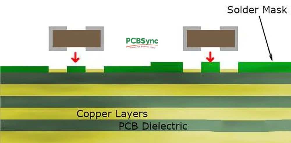
Solder Mask Clearance
The solder mask clearance (or swell) defines how much larger the mask opening is compared to the copper pad. Standard practice is 2-3 mils (50-75μm) per side.
Too small: The mask might cover pad edges, reducing solderable area
Too large: Risk of exposing adjacent traces or reducing insulation
Solder Mask Dam (Bridge) Width
The dam is the strip of mask between adjacent pads. Without it, solder can bridge between pins.
Green mask: Minimum 4 mils (0.1mm)
Other colors: Minimum 5 mils (0.127mm)
Fine-pitch BGAs: Consider solder mask defined (SMD) pads when dam width is impossible
SMD vs NSMD Pads
Solder Mask Defined (SMD): The mask opening is smaller than the copper pad. The mask overlaps the pad edges, defining the solderable area. Use this when you can’t achieve adequate dam width.
Non-Solder Mask Defined (NSMD): The mask opening is larger than the copper pad, exposing the entire pad plus clearance. This is the default for most components and allows larger solderable areas.
Via Tenting
Covering vias with solder mask (tenting) prevents solder from wicking down the hole during assembly and protects against contamination.
Vias with finished diameter ≤12 mils (0.3mm) tent reliably with LPI
Larger vias may need via filling or plugging for complete closure
Vias under BGA components should always be tented or filled
Common Solder Mask Defects and How to Avoid Them
Even with the best intentions, things can go wrong. Here are the issues I see most often and how to prevent them.
Solder Mask Misalignment
Symptoms: Mask covering parts of pads, or pads offset from their intended openings.
Causes: Registration errors during exposure, artwork misalignment, or substrate dimensional changes.
Prevention: Ensure design files use consistent registration marks. Work with manufacturers who have tight alignment tolerances. Add sufficient clearance.
Incomplete Coverage
Symptoms: Exposed copper in areas that should be masked, often visible as darker patches.
Causes: Surface contamination, inadequate mask application, or complex topography.
Prevention: Proper surface preparation, appropriate mask viscosity, and potentially multiple coat applications for heavy copper.
Delamination and Peeling
Symptoms: Mask lifting from the board, often discovered during or after soldering.
Causes: Poor adhesion due to contamination, under-curing, thermal stress, or incompatible flux chemistry.
Symptoms: Unintended solder connections between adjacent pads or traces.
Causes: Missing or insufficient solder mask dams, excessive solder paste, or damaged mask.
Prevention: Maintain minimum dam widths, verify mask integrity before assembly, optimize stencil design.
Solder Mask vs Paste Mask: Understanding the Difference
These two layers often confuse designers, but they serve completely different purposes in the manufacturing process.
Aspect
Solder Mask
Paste Mask (Stencil)
Purpose
Protects PCB, prevents solder bridges
Defines solder paste deposition areas
Permanent?
Yes, part of finished PCB
No, used to create stencil
Openings
Larger than or equal to pads
Often smaller than pads (paste reduction)
Components
All component types
SMD components only
The paste mask layer defines the stencil used during SMT assembly to apply solder paste. It’s typically sized smaller than the actual pad to control paste volume and prevent bridging.
Useful Resources and Standards
Here are the key references every PCB designer should have access to:
Industry Standards
IPC-SM-840: Qualification and Performance of Permanent Solder Mask
IPC-6012: Qualification and Performance Specification for Rigid Printed Boards
IPC-A-600: Acceptability of Printed Boards
IPC-J-STD-001: Requirements for Soldered Electrical and Electronic Assemblies
IPC-2221: Generic Standard on Printed Board Design
Green became the industry standard for several practical reasons: it provides optimal contrast for visual inspection without causing eye strain, offers the best resolution for fine solder mask dams (4 mils vs 5 mils for other colors), and benefits from decades of process refinement resulting in the lowest cost and highest reliability. The chemistry was also among the first to be perfected for photoimaging.
What is the standard solder mask thickness?
Typical solder mask thickness ranges from 12-75μm (0.5-3 mils), with 20-30μm being common for standard applications. The thickness varies based on copper weight, board topography, and application requirements. Per IPC-SM-840, the key requirement is achieving minimum 500 VDC per 25μm of dielectric strength rather than a specific thickness value.
Can you remove solder mask from a PCB?
Yes, solder mask can be removed for rework or repair using several methods: careful scraping with a fiberglass brush or exacto knife for small areas, chemical strippers formulated for solder mask removal, or abrasion with fine sandpaper. For production rework, UV-curable solder mask repair materials can be applied and cured to restore protection. However, removal should be a last resort as it can damage underlying copper.
What’s the difference between LPI and DFSM solder masks?
LPI (Liquid Photoimageable) mask is applied as a liquid via spray or curtain coating, making it ideal for complex surface topographies. DFSM (Dry Film Solder Mask) comes as a pre-made sheet that’s vacuum-laminated onto the board, providing perfectly uniform thickness. LPI is more economical and versatile for most applications, while DFSM excels in high-reliability applications requiring consistent dielectric properties or very fine-line spacing.
Does solder mask color affect PCB performance?
For most electrical applications, solder mask color has minimal impact on performance. However, there are practical differences: black masks absorb more heat (potentially affecting thermal management), white masks reflect light (beneficial for LED applications), and different colors have varying inspection characteristics. At high frequencies, the dielectric properties of the mask material matter more than the pigment color.
Wrapping Up
Solder mask might seem like a simple protective coating, but as we’ve explored, it’s a carefully engineered material that plays a critical role in PCB manufacturing and long-term reliability. Whether you’re designing a simple prototype or a high-density multilayer board for aerospace applications, understanding solder mask types, colors, thickness requirements, and design guidelines will help you create boards that manufacture reliably and perform as intended.
The key takeaways? Stick with green for most applications unless you have a specific reason to choose otherwise. Pay attention to solder mask clearances and dam widths in your designs. And work closely with your PCB manufacturer to ensure your design files meet their DFM requirements for solder mask.Got questions about solder mask for your specific application? Drop a comment below or reach out—I’m always happy to help fellow engineers navigate these details.
Inquire: Call 0086-755-23203480, or reach out via the form below/your sales contact to discuss our design, manufacturing, and assembly capabilities.
Quote: Email your PCB files to Sales@pcbsync.com (Preferred for large files) or submit online. We will contact you promptly. Please ensure your email is correct.
Notes: For PCB fabrication, we require PCB design file in Gerber RS-274X format (most preferred), *.PCB/DDB (Protel, inform your program version) format or *.BRD (Eagle) format. For PCB assembly, we require PCB design file in above mentioned format, drilling file and BOM. Click to download BOM template To avoid file missing, please include all files into one folder and compress it into .zip or .rar format.


