Inquire: Call 0086-755-23203480, or reach out via the form below/your sales contact to discuss our design, manufacturing, and assembly capabilities.
Quote: Email your PCB files to Sales@pcbsync.com (Preferred for large files) or submit online. We will contact you promptly. Please ensure your email is correct.
Notes: For PCB fabrication, we require PCB design file in Gerber RS-274X format (most preferred), *.PCB/DDB (Protel, inform your program version) format or *.BRD (Eagle) format. For PCB assembly, we require PCB design file in above mentioned format, drilling file and BOM. Click to download BOM template To avoid file missing, please include all files into one folder and compress it into .zip or .rar format.
When designing electronic circuits, choosing the right PCB type is crucial for project success. Single layer PCB, also known as single sided PCB, remains one of the most popular and cost-effective solutions in the electronics industry. As a PCB engineer with years of experience, I’ve seen how these boards continue to power countless devices despite the rise of more complex multilayer alternatives.
In this comprehensive guide, I’ll share everything you need to know about single layer PCBs, from their basic structure to advanced design considerations and real-world applications.
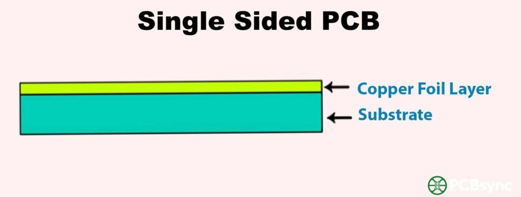
A single layer PCB is a printed circuit board featuring only one conductive copper layer on one side of an insulating substrate. This represents the simplest form of PCB construction, where all electrical connections and component traces are routed on a single plane.
The fundamental characteristic that defines single sided PCBs is their asymmetric design. Components typically mount on one side of the board while the copper traces that create electrical pathways exist on the opposite side. This straightforward architecture makes them ideal for low-density circuit designs where component count and routing complexity remain manageable.
Since their introduction in the 1950s, single layer PCBs have evolved significantly in manufacturing quality while maintaining their core simplicity. Today, they account for a substantial portion of global PCB production, particularly for consumer electronics and cost-sensitive applications.
Structure and Components of Single Sided PCB
Understanding the layer composition helps in making informed design decisions. A typical single layer PCB consists of four essential layers:
Substrate Layer
The substrate forms the foundation of the board, providing mechanical support and electrical insulation. FR-4 (Flame Retardant-4) is the industry standard material, composed of woven fiberglass cloth with epoxy resin binder. This material offers excellent dimensional stability, heat resistance up to 130°C, and superior mechanical strength.
Alternative substrate materials include:
CEM-1 and CEM-3: Cost-effective options using epoxy and fiberglass, popular in Asian markets
Phenolic resin: Budget-friendly but with lower heat resistance
Aluminum: Excellent for LED applications requiring superior heat dissipation
Polyimide: For flexible single layer PCBs requiring bendability
Conductive Copper Layer
The copper layer typically ranges from 1 oz to 3 oz thickness (35-105 microns). This layer gets etched during manufacturing to create the circuit traces, pads, and connection points. Thicker copper supports higher current capacity but increases manufacturing costs and may complicate fine-pitch routing.
Solder Mask Layer
This protective coating, usually green but available in red, blue, white, yellow, or black, serves multiple critical functions. It prevents oxidation of copper traces, reduces the risk of solder bridges during assembly, and provides electrical insulation. The solder mask gets selectively removed only at component pads where soldering occurs.
Silkscreen Layer
The final layer contains white (or contrasting color) printed text, reference designators, component outlines, polarity markers, and test points. This layer is invaluable during assembly, testing, and field service operations.
Key Advantages of Single Layer PCB
From an engineering perspective, single sided PCBs offer several compelling benefits:
Cost-Effectiveness
Manufacturing costs remain significantly lower than double-sided or multilayer alternatives. With only one copper layer to process, material consumption drops substantially. For high-volume production runs, this cost advantage multiplies exponentially. Based on current industry data, single layer boards cost approximately 40-60% less than comparable double-sided designs.
The production workflow requires fewer steps, reducing cycle time and increasing yield rates. There’s no need for via drilling, plating through-holes for interlayer connections, or complex layer alignment. This simplicity translates to faster turnaround times, with prototype boards often available within 24-48 hours.
Design Transparency
All traces remain visible on one side, making visual inspection, troubleshooting, and repairs straightforward. When debugging fails in the field, technicians can quickly trace signals without specialized equipment or documentation.
High Reliability
With fewer processing steps and no interlayer connections, potential failure points decrease. Single layer boards demonstrate excellent long-term reliability in stable operating environments. The absence of vias eliminates common failure modes like barrel cracking and pad separation.
Ease of Prototyping
For hobbyists and engineers validating new concepts, single sided PCBs can even be manufactured using DIY methods like toner transfer or photoresist processes. This accessibility makes them perfect for educational purposes and rapid iteration cycles.
Limitations and Disadvantages
Despite their advantages, single layer PCBs have inherent limitations that engineers must consider:
Restricted Routing Density
With only one copper layer available, trace routing becomes challenging as component count increases. Crossing traces is impossible without using jumper wires or zero-ohm resistors, which add manual assembly steps and potential reliability concerns.
Limited Component Density
The single-sided nature requires more board area to accommodate the same number of components compared to double-sided designs. This makes miniaturization difficult and may increase overall product size.
No Ground Plane
Single layer boards cannot incorporate continuous ground planes, which provide superior electromagnetic compatibility (EMC), reduced crosstalk, and better high-frequency performance. This limitation restricts their use in RF applications and high-speed digital circuits.
Power Handling Constraints
Without the ability to dedicate entire layers to power distribution, single sided PCBs struggle with high-current applications unless trace widths increase substantially, consuming precious routing space.
Manufacturing Process of Single Layer PCB
Understanding the manufacturing workflow helps designers optimize their layouts for manufacturability. Here’s the step-by-step process I follow:
Step 1: Design and CAD Layout
Circuit design begins in specialized PCB design software like Altium Designer, KiCad, Eagle, or EasyEDA. The schematic gets converted into a physical layout where component placement and trace routing occur. Design Rule Checks (DRC) ensure the layout meets manufacturing capabilities.
Step 2: Substrate Preparation
Raw copper-clad laminate arrives from material suppliers with copper foil already bonded to one side. The substrate gets cut to panel size and thoroughly cleaned to remove contaminants that could affect subsequent processing.
Step 3: Photoresist Application and Exposure
A photosensitive resist layer gets applied to the copper surface. The circuit pattern, generated from Gerber files, gets transferred using UV light exposure through a photomask. Areas exposed to UV light harden while unexposed regions remain soluble.
Step 4: Developing and Etching
The board passes through a developer solution that washes away unexposed photoresist, revealing bare copper in areas to be removed. Next, chemical etchant (typically ferric chloride or ammonium persulfate) dissolves the exposed copper, leaving only the protected circuit pattern.
Step 5: Drilling
CNC drilling machines create holes for through-hole component leads and mechanical mounting points. Hole sizes typically range from 0.3mm to 6.5mm depending on component requirements. Modern equipment achieves positional accuracy within ±0.075mm.
Step 6: Surface Finish Application
The exposed copper receives a surface finish to prevent oxidation and ensure solderability. Common finishes include:
HASL (Hot Air Solder Leveling): Cost-effective, good shelf life
Immersion Silver or Tin: Good middle-ground options
Step 7: Solder Mask and Silkscreen
Solder mask ink gets screen-printed or photo-imaged onto the board, then cured. Silkscreen legend printing follows, adding component identifiers and other markings.
Step 8: Testing and Quality Control
Electrical testing verifies continuity and isolation. Visual inspection catches cosmetic defects. Boards passing all checks get routed from production panels and prepared for shipment.
Design Considerations for Single Sided PCB
Successful single layer board design requires attention to specific guidelines:
Trace Width and Spacing
Minimum trace width depends on copper thickness and current requirements. For 1 oz copper, I recommend:
Signal traces: 0.15mm minimum (6 mils)
Power traces: Calculate based on current using IPC-2221 standards
Trace spacing: 0.15mm minimum for standard applications
Online trace width calculators help determine appropriate dimensions based on current load and acceptable temperature rise.
Component Placement Strategy
Place components to minimize trace crossings. Group related components together and orient them consistently. Through-hole components work particularly well with single sided designs since their leads naturally extend through the board.
Jumper Wire Management
When trace crossing becomes unavoidable, plan jumper wire locations carefully. Using zero-ohm resistors provides a cleaner solution than manual wiring, though it increases component cost slightly.
Ground Distribution
Without a ground plane, create a ground “grid” or “star” pattern with appropriately wide traces. Connect all ground points systematically to minimize ground loops and voltage drops.
Thermal Considerations
For components generating significant heat, ensure adequate copper area beneath them for heat dissipation. On aluminum-backed single sided PCBs, thermal vias can transfer heat to the metal backing.
Design for Manufacturability (DFM)
Leave adequate clearance between components and board edges (typically 5mm minimum). Avoid acute angles in traces; use 45-degree or curved corners instead of 90-degree bends. Provide tooling holes for manufacturing fixtures.
Applications and Use Cases
Single layer PCBs excel in specific application domains:
Consumer Electronics
Remote controls for televisions and air conditioners
Basic calculators and timers
LED lighting controllers and drivers
Radio receivers and simple audio circuits
Toys and electronic games
Power Supplies
Linear power supplies with low component count
Simple switch-mode power supplies (low frequency)
Battery charging circuits
Power distribution boards
Automotive Applications
Interior lighting controllers
Basic sensor interfaces
Relay driver boards
Warning indicator panels
Industrial Equipment
Timer and relay control panels
Simple human-machine interfaces
Sensor breakout boards
Basic motor controllers
Educational and Prototyping
Learning kits for electronics education
Proof-of-concept prototypes
Development boards for simple microcontroller projects
Single Layer PCB vs Double Layer PCB
Understanding when to choose single over double layer boards is crucial:
Design Complexity
Single layer boards suit circuits with fewer than 20-30 components and straightforward routing. Double-sided designs handle 50-100+ components with complex interconnections.
Cost Comparison
Single sided PCBs cost 40-60% less in prototype quantities. However, this gap narrows in high-volume production where setup costs dominate. For many manufacturers, double-sided boards cost only 10-20% more at volumes above 10,000 units.
Performance Characteristics
Double-sided boards with ground planes offer superior signal integrity, EMI performance, and power distribution. Single layer boards suffice for low-frequency applications under 1 MHz.
Assembly Considerations
Single sided boards support wave soldering efficiently since components mount on one side with solder joints on the other. Double-sided boards may require selective soldering or two-pass reflow processes.
Cost Analysis and Pricing Factors
Several factors influence single layer PCB pricing:
Board Size
Larger boards consume more material and panel space, increasing costs proportionally. Optimizing board dimensions can yield significant savings.
Quantity
Unit costs drop dramatically with volume. A prototype board costing $50 individually might cost $2-5 each at 1000 units.
Surface Finish
HASL represents the most economical choice at $0.50-1.00 per board. ENIG adds $2-5 per board but provides superior performance.
Turnaround Time
Standard lead times (7-10 days) offer best pricing. Express services (24-48 hours) typically cost 2-3 times more.
Copper Thickness
Standard 1 oz copper includes no premium. Heavy copper (2-3 oz) increases costs by 20-40%.
Current market pricing for single layer PCBs ranges from $0.10 to $5.00 per board depending on specifications and quantity, making them highly attractive for cost-sensitive applications.
Quality Standards and Certifications
Professional single layer PCB manufacturing adheres to international standards:
IPC-A-600: Acceptability criteria for printed boards
IPC-6012: Qualification and performance specifications
IPC-2221: Generic standard on printed board design
ISO 9001: Quality management system certification
UL 94V-0: Flammability rating for materials
RoHS: Restriction of hazardous substances compliance
Reputable manufacturers maintain these certifications and provide test reports with each production batch.
Future Outlook for Single Layer PCB Technology
Despite advancing technology trends toward miniaturization and higher complexity, single layer PCBs maintain relevance for several reasons:
The Internet of Things (IoT) expansion creates demand for simple, low-cost sensor nodes and basic control circuits. Many IoT edge devices require minimal processing power and simple circuits perfectly suited to single sided construction.
Sustainability concerns favor simpler designs with less material consumption and easier recycling. Single layer boards use fewer resources and chemicals during manufacturing compared to complex multilayer alternatives.
Educational applications continue growing as electronics education expands globally. Single sided PCBs remain ideal teaching tools due to their transparency and accessibility.
However, I expect gradual technology improvements rather than revolutionary changes. Enhanced materials, finer resolution photolithography, and better surface finishes will incrementally improve single layer PCB capabilities while maintaining their core advantages.
Frequently Asked Questions (FAQs)
1. Can single layer PCBs be used for Arduino or Raspberry Pi projects?
Yes, absolutely. Single layer PCBs work excellently for Arduino and Raspberry Pi shield designs, breakout boards, and peripheral circuits. However, the main processor boards themselves use multilayer designs due to their complexity. For sensor interfaces, LED drivers, relay controllers, and similar add-on circuits, single sided boards provide perfect solutions. I’ve designed dozens of Arduino shields using single layer construction with great success.
2. What is the minimum trace width and spacing achievable on single layer PCBs?
Standard manufacturing capabilities support trace widths and spacing down to 0.15mm (6 mils) reliably. Some specialized manufacturers offer 0.1mm (4 mils) minimum features, though this increases costs and reduces yield. For most applications, I recommend designing with 0.2mm (8 mils) or larger features to maximize manufacturability and reduce production costs. Always consult your chosen manufacturer’s capabilities before finalizing designs.
3. How do I handle crossed traces on a single sided PCB?
You have three practical solutions: First, use zero-ohm resistors as jumpers—these surface-mount components bridge traces at crossing points. Second, design jumper wire connections using through-hole pads where manual wiring occurs during assembly. Third, re-route your circuit to eliminate crossings through creative layout. The first option provides the cleanest, most reliable solution for production quantities, while the second works acceptably for prototypes and low-volume production.
4. Is it possible to manufacture flexible single layer PCBs?
Yes, flexible single sided PCBs are quite common. They use polyimide (PI) substrate material instead of rigid FR-4. The manufacturing process remains similar, though handling requires special care due to material flexibility. Flexible single layer boards excel in applications requiring movement, tight bending radii, or three-dimensional packaging. Common applications include flexible circuits in cameras, printers, and medical devices. Expect 30-50% higher costs compared to rigid equivalents due to specialized materials and handling requirements.
5. What maximum current can single layer PCB traces handle?
Current capacity depends on three primary factors: copper thickness, trace width, and acceptable temperature rise. Using IPC-2221 standards, a 1mm wide trace with 1 oz copper can safely carry approximately 2-3 amps with a 10°C temperature rise. For 2 oz copper, this increases to 3-4 amps. For higher currents, either increase trace width proportionally or use heavier copper. Online trace width calculators provide precise values for your specific requirements. In power applications, I always recommend adding 20-30% margin beyond calculated minimums for long-term reliability.
Conclusion
Single layer PCBs represent a time-tested, cost-effective solution for countless electronic applications. While they may not suit every project, their simplicity, affordability, and reliability make them indispensable in modern electronics manufacturing.
As a PCB engineer, I continue recommending single sided designs whenever project requirements align with their capabilities. Understanding when to choose single layer construction versus more complex alternatives separates good designers from great ones. By applying the principles and guidelines outlined in this guide, you’ll make informed decisions that optimize both performance and cost for your specific application needs.
Whether you’re designing your first PCB or optimizing production costs for an existing product, single layer PCBs deserve serious consideration. Their proven track record spanning over 70 years demonstrates enduring value in our rapidly evolving industry.
Inquire: Call 0086-755-23203480, or reach out via the form below/your sales contact to discuss our design, manufacturing, and assembly capabilities.
Quote: Email your PCB files to Sales@pcbsync.com (Preferred for large files) or submit online. We will contact you promptly. Please ensure your email is correct.
Notes: For PCB fabrication, we require PCB design file in Gerber RS-274X format (most preferred), *.PCB/DDB (Protel, inform your program version) format or *.BRD (Eagle) format. For PCB assembly, we require PCB design file in above mentioned format, drilling file and BOM. Click to download BOM template To avoid file missing, please include all files into one folder and compress it into .zip or .rar format.


