Inquire: Call 0086-755-23203480, or reach out via the form below/your sales contact to discuss our design, manufacturing, and assembly capabilities.
Quote: Email your PCB files to Sales@pcbsync.com (Preferred for large files) or submit online. We will contact you promptly. Please ensure your email is correct.
Notes: For PCB fabrication, we require PCB design file in Gerber RS-274X format (most preferred), *.PCB/DDB (Protel, inform your program version) format or *.BRD (Eagle) format. For PCB assembly, we require PCB design file in above mentioned format, drilling file and BOM. Click to download BOM template To avoid file missing, please include all files into one folder and compress it into .zip or .rar format.
As a PCB engineer who has spent over a decade working with various soldering technologies, I can tell you that selective soldering has fundamentally changed how we approach mixed-technology board assembly. When traditional wave soldering started damaging our heat-sensitive SMT components and hand soldering became too slow for production volumes, selective soldering emerged as the solution that bridged the gap.
In this comprehensive guide, I’ll walk you through everything you need to know about selective soldering—from the fundamental process steps to equipment selection and troubleshooting common defects. Whether you’re evaluating selective soldering for your production line or looking to optimize an existing process, this guide will give you the practical knowledge you need.
Selective soldering is an automated soldering process designed specifically for soldering through-hole (THT) components on printed circuit boards where traditional wave soldering isn’t practical. Unlike wave soldering, which exposes the entire bottom side of a PCB to molten solder, selective soldering applies solder only to designated areas using a programmable miniature solder wave or fountain.
The process emerged in the 1980s as surface mount technology (SMT) began dominating PCB assembly. As boards became increasingly populated with SMT components on both sides, manufacturers needed a way to solder the remaining through-hole components without damaging nearby surface mount parts. Selective soldering filled this critical gap.
Selective Soldering vs Wave Soldering: Key Differences
Understanding the distinction between these two processes is essential for making the right choice for your application:
Feature
Selective Soldering
Wave Soldering
Solder Application
Targeted to specific joints only
Entire board bottom exposed
Heat Exposure
Minimal, localized heating
Board-wide thermal stress
Flux Application
Precise, drop-jet or micro-spray
Full board flux coating
Throughput
Lower (sequential soldering)
Higher (all joints at once)
Tooling Required
Minimal or none (toolless)
Pallets/carriers often needed
Best For
Mixed-technology boards, low-medium volume
High-volume, through-hole only boards
Setup Time
Quick program changes
Carrier/pallet changes needed
Material Waste
Lower solder and flux consumption
Higher consumption
The fundamental difference lies in how heat is managed. In wave soldering, the PCB’s thermal mass must absorb significant heat energy across the entire surface. With selective soldering, only the immediate area around each solder joint experiences elevated temperatures, protecting sensitive components just millimeters away.
How the Selective Soldering Process Works
The selective soldering process consists of four critical stages, each requiring precise control to achieve reliable solder joints. Let me break down each step based on what actually happens on the production floor.
Step 1: Flux Application
Flux application is arguably the most critical step in selective soldering. The flux serves multiple purposes: it removes oxides from the pad and component lead surfaces, prevents re-oxidation during heating, and promotes proper wetting of the solder.
There are two primary flux application methods:
Spray Fluxing: An atomized flux spray is applied to specific areas. This method covers larger areas quickly but with less precision.
Drop-Jet Fluxing: Individual droplets of flux are precisely deposited onto each solder joint location. This is the preferred method for most selective soldering applications because it eliminates flux contamination on adjacent components.
The flux quantity matters significantly. Too little flux results in poor wetting and incomplete joints. Too much flux can spread to nearby SMT components and cause reliability issues if it remains un-activated after soldering. A typical flux deposit diameter is around 2mm minimum, with placement accuracy of ±0.5mm.
Step 2: Preheating
Before the board reaches the solder wave, it must be preheated to achieve several objectives:
Evaporate flux solvents
Activate flux chemistry
Reduce thermal shock when the board contacts molten solder
Minimize the heat energy the solder wave must supply
Typical preheat temperatures range from 80°C to 130°C on the board’s top side. The exact temperature depends on the flux manufacturer’s specifications—exceeding the recommended maximum can exhaust the flux before soldering completes, leading to defects like bridging and flags.
Bottom-side infrared (IR) preheaters are most common, though some machines incorporate top-side heating for boards with high thermal mass components. The goal is to supply approximately 50% of the total thermal energy through preheating, with the solder wave providing the remainder.
Step 3: Soldering (Dip and Drag Methods)
The actual soldering occurs through two primary techniques:
Dip Soldering: The PCB is lowered onto a miniature solder wave, held for a programmed dwell time (typically 2-5 seconds), then lifted away. This method works well for:
Single components with multiple pins
Connector rows
Areas where multiple joints can be soldered simultaneously
Drag Soldering: The solder wave moves along a row of pins (or the board moves over the wave), soldering each joint in sequence. Drag soldering excels at:
Long connector rows
Densely packed through-hole areas
Applications requiring precise solder volume control
Most modern selective soldering machines support both methods and can switch between them within a single program. The choice depends on component layout and the keep-out areas around each solder joint.
Typical Process Parameters:
Parameter
Lead-Free (SAC305)
SnPb (63/37)
Solder Pot Temperature
275°C – 300°C
250°C – 260°C
Preheat Temperature (top side)
100°C – 130°C
80°C – 120°C
Contact Time (dip)
3 – 5 seconds
2 – 4 seconds
Drag Speed
3 – 10 mm/s
5 – 15 mm/s
Step 4: Cooling
After soldering, proper cooling is essential to form reliable metallurgical bonds. The cooling phase must be controlled to:
Allow solder joints to solidify without thermal shock
Prevent cracking from differential thermal expansion
Stabilize the intermetallic compound (IMC) layer
Most selective soldering systems incorporate a cooling zone or allow boards to cool gradually on the exit conveyor. Forced air cooling is sometimes used for higher throughput, but the cooling rate must remain within acceptable limits to avoid joint defects.
Types of Selective Soldering Systems
Selective soldering equipment comes in several configurations, each suited to different production requirements.
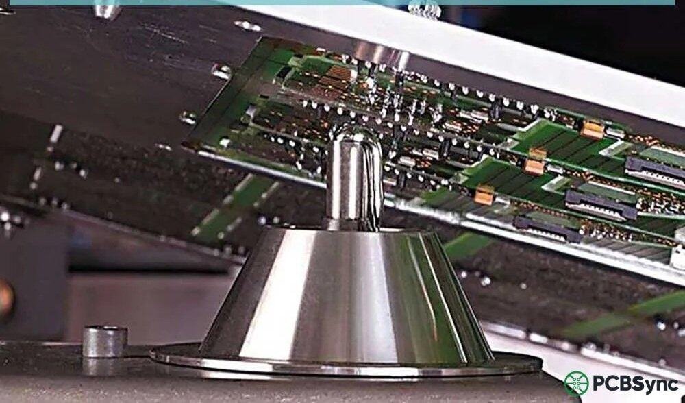
Miniature Wave Selective Solder Fountain
This is the most common and versatile selective soldering method. A small, programmable nozzle (typically 2.5mm to 20mm diameter) creates a solder fountain that can be precisely positioned under any point on the board.
Advantages:
Toolless operation—no custom pallets required
Maximum flexibility for different board designs
Individual parameter control for each solder joint
Quick changeover between products
Considerations:
Slower than mass soldering methods
Best suited for low to medium volume production
Multi-Wave (Dip) Soldering
Multi-wave systems use custom nozzle plates with multiple solder fountains arranged to match specific component layouts. The entire board is dipped into all fountains simultaneously.
Advantages:
Higher throughput than single-nozzle systems
All joints soldered at once
Consistent results across all joints
Considerations:
Requires custom tooling for each product
Less flexible for product changeovers
Higher initial tooling cost
Laser Selective Soldering
A newer technology that uses laser energy to directly heat and melt solder onto each joint. The system imports CAD data and positions the laser precisely over each solder point.
Advantages:
No physical contact with the board
Minimal thermal stress
Extremely precise positioning
Fast cycle times (approximately 1 second per joint)
No solder masks or stencils required
Considerations:
Higher equipment cost
May require solder preforms or paste
Limited to certain joint configurations
Selective Aperture Wave Soldering
This hybrid approach uses traditional wave soldering equipment with custom pallets that mask off SMT components, exposing only the through-hole areas to the wave.
Advantages:
Uses existing wave solder equipment
High throughput for suitable applications
Good for high-volume production
Considerations:
Requires custom pallets for each product
Minimum clearance requirements between THT and SMT
Not suitable for densely populated boards
Selective Soldering Equipment Components
Understanding the key components of a selective soldering machine helps in both equipment selection and process optimization.
Solder Pot and Nozzle System
The solder pot maintains a reservoir of molten solder, typically holding 10-50 kg depending on the machine size. Electromagnetic pumps are preferred over mechanical pumps because they:
Produce minimal dross (no moving parts in the solder)
Provide extremely stable flow rates
Allow precise wave height control
Require less maintenance
Nozzle selection depends on the solder joint geometry and surrounding component clearances. Common nozzle diameters range from 2.5mm for fine-pitch work to 20mm for large connectors.
Nozzle Type
Typical Diameter
Best Applications
Standard Round
3mm – 6mm
General purpose, single pins
Large Round
8mm – 20mm
Connectors, multi-pin dipping
Wettable
Various
Lead-free, improved wetting
Non-Wettable
Various
SnPb, reduced bridging
Custom Rectangular
Variable
Specific connector footprints
Flux Application System
Drop-jet fluxers use piezoelectric or solenoid-driven dispensing heads to deposit precise flux droplets. Key specifications include:
Droplet volume control
X-Y positioning accuracy
Deposit diameter consistency
Nozzle anti-clog features
Preheating System
Bottom-side IR emitters are standard, with optional top-side heaters for high-mass applications. Preheater specifications to consider:
Heating power (typically 1-3 kW per zone)
Temperature uniformity across the board
Closed-loop temperature control
Multiple zone capability
Motion Control and Programming
Modern selective soldering machines feature:
X-Y-Z servo-driven positioning systems
Gerber data import for programming
Teach programming with vision systems
Program libraries for product families
Real-time process monitoring
Nitrogen Inerting System
Most production selective soldering is performed in a nitrogen atmosphere. Nitrogen provides several critical benefits:
Oxidation Prevention: Molten solder oxidizes rapidly in air, forming dross on the wave surface and degrading wetting. Nitrogen atmospheres with less than 50 ppm oxygen dramatically reduce oxidation.
Improved Wetting: Lead-free alloys in particular benefit from nitrogen inerting, with wetting angles improving significantly compared to air atmosphere.
Reduced Dross Formation: Nitrogen can reduce dross by 80-90%, lowering solder consumption and maintenance requirements.
Better Joint Appearance: Joints soldered in nitrogen have brighter, smoother surfaces with improved cosmetic appearance.
Nitrogen consumption varies by machine design, typically ranging from 10-30 m³/hour. Many facilities use nitrogen generators rather than bulk liquid nitrogen for cost efficiency.
PCB Design Guidelines for Selective Soldering
Good PCB design is essential for successful selective soldering. Here are the critical considerations I’ve learned from working with countless board designs.
Keep-Out Zone Requirements
The most important design consideration is maintaining adequate clearance between through-hole solder joints and adjacent SMT components.
Nozzle Size
Minimum Keep-Out Distance
3mm nozzle
3.5mm – 4.0mm from pad edge
6mm nozzle
5.0mm – 5.5mm from pad edge
10mm nozzle
7.0mm – 8.0mm from pad edge
These distances account for the nozzle body plus the flowing solder wave. Components within this zone risk solder contact or excessive heat exposure.
Component Lead Length
Lead length significantly affects selective soldering quality:
Optimal length: 1.0mm – 1.5mm below the board surface
Minimum length: 0.5mm
Maximum length: 2.0mm (longer leads increase bridging risk)
Clinched leads should not extend beyond the pad boundaries, as this can interfere with nozzle positioning.
Pad and Via Design
Design recommendations for THT pads in selective soldering applications:
Maintain consistent pad sizes within component groups
Provide thermal relief connections to ground planes
Avoid filled vias within pad areas
Ensure annular rings meet IPC specifications
Consider solder mask defined pads for tight-pitch applications
Component Spacing on Bottom Side
For the board’s bottom (solder) side:
Maximum component height: typically 10mm (standard nozzle height is 55mm)
Maintain 3mm minimum from board edge
Avoid placing tall components near through-hole solder joints
Common Selective Soldering Defects and Troubleshooting
Even with proper setup, defects can occur. Here’s how to identify and correct the most common issues.
Solder Bridging
Symptoms: Solder connects adjacent pins or pads
Common Causes:
Insufficient flux activity
Poor nozzle peel-off movement
Excessive contact time
Low solder temperature
Contaminated solder
Solutions:
Verify flux is properly activated (check preheat temperature)
Optimize exit angle and speed when leaving the wave
Reduce dwell time
Check nitrogen purity (if using inert atmosphere)
Reduce lead length if exceeding 1.5mm
Insufficient Fill (Incomplete Hole Fill)
Symptoms: Solder doesn’t wet up through the plated hole
Common Causes:
Insufficient thermal energy
Poor flux coverage
Oxidized board or leads
Inadequate contact time
Large thermal mass components
Solutions:
Increase preheat temperature
Verify flux is reaching the joint
Check incoming board quality
Extend contact time
Use larger nozzle for better thermal transfer
Solder Balls
Symptoms: Small solder spheres on the board surface
Common Causes:
Flux spattering from rapid heating
Moisture in the flux
Excessive flux quantity
Inadequate preheating
Solutions:
Increase preheat time or temperature
Check flux storage and handling
Reduce flux volume
Verify flux is fully activated before soldering
Flags and Icicles
Symptoms: Solder projections extending from joints
Common Causes:
Exhausted flux activity
Poor wave separation
Solder temperature too low
Excessive oxidation
Solutions:
Reduce preheat to maintain flux activity
Adjust nozzle exit movement
Increase solder temperature
Verify nitrogen flow and purity
Troubleshooting Reference Table
Defect
First Check
Second Check
Third Check
Bridging
Lead length
Peel-off speed
Flux activity
Poor fill
Preheat temp
Contact time
Nozzle size
Solder balls
Preheat temp
Flux quantity
Flux quality
Flags/icicles
Solder temp
N2 purity
Flux type
Dull joints
Solder temp
Cooling rate
Alloy contamination
Industry Applications for Selective Soldering
Selective soldering has become indispensable across multiple industries where reliability and precision are paramount.
Automotive Electronics
Modern vehicles contain dozens of electronic control units (ECUs) that must withstand extreme temperature variations, vibration, and decades of operation. Selective soldering is used for:
Engine control modules
Transmission controllers
Safety system electronics
Infotainment systems
EV battery management systems
Charging infrastructure
The automotive industry’s zero-defect requirements make selective soldering’s precision and repeatability essential.
Medical Devices
Medical electronics demand the highest reliability standards. Selective soldering applications include:
Patient monitoring equipment
Diagnostic instruments
Implantable device components
Laboratory analyzers
Imaging system electronics
The process’s ability to protect heat-sensitive components while ensuring consistent joint quality meets FDA and ISO 13485 requirements.
Aerospace and Defense
Avionics and military electronics operate in extreme environments and must function flawlessly. Applications include:
Flight control systems
Communication equipment
Radar and sensor systems
Navigation electronics
Satellite components
Many aerospace applications still require SnPb solder for reliability, which selective soldering handles seamlessly alongside lead-free requirements.
Telecommunications and Networking
5G infrastructure and data center equipment rely on selective soldering for:
High-frequency RF modules
Power distribution boards
Network switching equipment
Fiber optic transceivers
Industrial Automation
Rugged industrial electronics benefit from selective soldering’s precision:
PLC controllers
Motor drives
Sensor interfaces
HMI displays
Advantages of Selective Soldering
After working with selective soldering for years, I’ve identified the key benefits that make this technology worth the investment:
Precision and Repeatability
Unlike hand soldering, where quality depends on operator skill and fatigue, selective soldering delivers identical results joint after joint. Programmed parameters ensure every solder joint receives the exact same flux quantity, preheat profile, and solder contact time. This consistency is critical for meeting Class 2 and Class 3 IPC standards.
Protection of Heat-Sensitive Components
Modern PCBs often contain components with maximum temperature ratings below wave soldering temperatures. By heating only the immediate joint area, selective soldering protects:
Temperature-sensitive ICs and modules
Pre-programmed microcontrollers
Batteries and supercapacitors
Plastic housings and connectors
Previously soldered SMT components
Reduced Material Waste
Selective soldering uses solder and flux only where needed. Compared to wave soldering, typical savings include:
50-70% reduction in flux consumption
30-50% reduction in solder usage
Elimination of wave solder pallets and carriers
Reduced cleaning requirements
Lower Defect Rates
The controlled nature of selective soldering significantly reduces common defects. Production data from multiple facilities shows:
Bridging defects reduced by 80% versus wave soldering
First-pass yield improvements of 5-15%
Rework rates typically below 0.5%
Process Documentation and Traceability
Modern selective soldering systems log every parameter for every board, providing complete traceability for quality assurance and root cause analysis when issues arise.
Equipment Manufacturers and Resources
Several manufacturers lead the selective soldering equipment market:
Manufacturer
Notable Products
Strengths
Ersa (Kurtz)
VERSAFLOW series
Modular inline systems, multi-wave
Nordson SELECT
Cerno, Integra series
Synchro motion technology
Pillarhouse
Orissa series
UK-based, diverse lineup
DDM Novastar
SL series
Cost-effective, quick delivery
Hentec/RPS
Various
Robotic precision systems
SEHO
SelectLine
German engineering
I.C.T
Various
Cost-competitive solutions
Useful Resources and Downloads
Industry Standards:
IPC J-STD-001: Requirements for Soldered Electrical and Electronic Assemblies
IPC-A-610: Acceptability of Electronic Assemblies
IPC-7530: Guidelines for Temperature Profiling for Mass Soldering
Technical References:
SMTA (Surface Mount Technology Association): Technical papers and webinars
IPC (Association Connecting Electronics Industries): Standards and training
Equipment manufacturer training programs
Process Monitoring Tools:
SolderStar WaveShuttle: Thermal profiling for selective soldering
Datapaq SelectivePaq: Process verification system
Frequently Asked Questions (FAQs)
What is the difference between selective soldering and wave soldering?
The fundamental difference is how solder is applied. Wave soldering passes the entire board bottom over a large wave of molten solder, soldering all through-hole joints simultaneously. Selective soldering uses a small, programmable solder fountain that targets only specific joints, leaving the rest of the board untouched. This makes selective soldering ideal for mixed-technology boards with both SMT and through-hole components, as it prevents heat damage to nearby surface mount parts.
What temperature should selective soldering be set at?
For lead-free solder alloys like SAC305, solder pot temperatures typically range from 275°C to 300°C. Traditional tin-lead (SnPb) solder operates at lower temperatures, around 250°C to 260°C. Preheat temperatures on the board’s top side should reach 100°C to 130°C for lead-free and 80°C to 120°C for SnPb. The exact settings depend on board thermal mass, component requirements, and flux specifications. Always start with manufacturer recommendations and adjust based on results.
When should I choose selective soldering over hand soldering?
Selective soldering becomes advantageous when you have more than a few through-hole joints per board and need consistent, repeatable quality. Typical break-even points are around 10-20 through-hole components per board or production volumes exceeding 50-100 boards per day. Beyond quality and speed, selective soldering reduces labor costs, minimizes operator-dependent variability, and provides documented process control that hand soldering cannot match.
What is the minimum keep-out distance for selective soldering?
The minimum distance between a through-hole pad edge and adjacent SMT components depends on nozzle size. For a typical 3mm nozzle, maintain at least 3.5mm to 4.0mm clearance. Larger nozzles require proportionally more space—an 8mm nozzle needs about 6mm clearance. These distances account for the nozzle body plus the flowing solder wave. Components closer than these minimums risk solder contact or thermal damage.
Can selective soldering work with lead-free solder?
Yes, selective soldering works exceptionally well with lead-free alloys. In fact, the process’s precise temperature control and nitrogen inerting capabilities make it particularly suited for lead-free soldering, which is more challenging than traditional SnPb due to higher melting points and reduced wetting. Lead-free selective soldering requires higher solder temperatures (275°C-300°C), longer contact times, and often nitrogen atmospheres to prevent oxidation and ensure proper wetting.
Conclusion
Selective soldering has evolved from a niche process to an essential technology for modern electronics manufacturing. Its ability to precisely solder through-hole components while protecting sensitive SMT parts makes it indispensable for mixed-technology boards across automotive, medical, aerospace, and industrial applications.
The keys to successful selective soldering implementation are understanding the process fundamentals, designing boards with selective soldering in mind, selecting appropriate equipment for your production requirements, and developing robust process parameters through systematic optimization.
Whether you’re considering selective soldering for a new production line or looking to improve an existing process, the investment in proper equipment, training, and process development pays dividends in quality, reliability, and manufacturing efficiency.
For more information on implementing selective soldering in your facility, consult with equipment manufacturers who can provide application-specific guidance based on your product requirements and production volumes. The technology continues advancing rapidly, with newer systems offering improved throughput, enhanced process monitoring, and greater automation capabilities that make selective soldering more accessible than ever.
Inquire: Call 0086-755-23203480, or reach out via the form below/your sales contact to discuss our design, manufacturing, and assembly capabilities.
Quote: Email your PCB files to Sales@pcbsync.com (Preferred for large files) or submit online. We will contact you promptly. Please ensure your email is correct.
Notes: For PCB fabrication, we require PCB design file in Gerber RS-274X format (most preferred), *.PCB/DDB (Protel, inform your program version) format or *.BRD (Eagle) format. For PCB assembly, we require PCB design file in above mentioned format, drilling file and BOM. Click to download BOM template To avoid file missing, please include all files into one folder and compress it into .zip or .rar format.


