Inquire: Call 0086-755-23203480, or reach out via the form below/your sales contact to discuss our design, manufacturing, and assembly capabilities.
Quote: Email your PCB files to Sales@pcbsync.com (Preferred for large files) or submit online. We will contact you promptly. Please ensure your email is correct.
Notes: For PCB fabrication, we require PCB design file in Gerber RS-274X format (most preferred), *.PCB/DDB (Protel, inform your program version) format or *.BRD (Eagle) format. For PCB assembly, we require PCB design file in above mentioned format, drilling file and BOM. Click to download BOM template To avoid file missing, please include all files into one folder and compress it into .zip or .rar format.
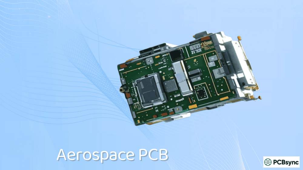
After fifteen years designing PCBs for aerospace applications, I’ve learned that satellite PCB design is fundamentally different from any terrestrial electronics work. You’re not just building a circuit board—you’re engineering a system that must survive the violence of launch, operate flawlessly in the vacuum of space, and withstand radiation bombardment for years without any possibility of repair.
This guide distills the critical requirements every engineer needs to understand when designing satellite PCBs, whether you’re working on a multi-million dollar GEO communications satellite or a university CubeSat project. I’ve seen projects fail because teams underestimated even one of these factors, so let’s get into the details.
Understanding the Space Environment for Satellite PCB Design
Before diving into specific design requirements, you need to understand what your satellite PCB will actually face. Space isn’t just cold and empty—it’s actively hostile to electronics in ways that aren’t immediately obvious.
Extreme Temperature Cycling in Orbit
Satellites experience temperature swings that would destroy any commercial electronics. In low Earth orbit (LEO), your PCB might cycle between -150°C in shadow and +150°C in direct sunlight—every 90 minutes. That’s roughly 5,800 thermal cycles per year. GEO satellites face even more extreme conditions, with temperatures ranging from -200°C to +200°C depending on orientation and eclipse periods.
These temperature swings create mechanical stress through differential thermal expansion. When your copper traces expand at a different rate than your substrate material, something has to give. Over thousands of cycles, even microscopic CTE mismatches can cause trace cracking, via failures, or delamination.
The radiation environment in space comes from three primary sources: galactic cosmic rays, solar particle events, and trapped radiation in the Van Allen belts. Each presents different challenges for your satellite PCB design.
Total Ionizing Dose (TID) represents cumulative radiation damage over your mission lifetime. For a typical LEO satellite on a 5-year mission, you might see 10-30 krad(Si). GEO missions can experience 50-100 krad or more. TID causes gradual degradation—increased leakage currents, threshold voltage shifts, and eventual component failure.
Single Event Effects (SEE) are more insidious. A single high-energy particle can cause bit flips in memory (SEU), temporary circuit upset (SET), or permanent damage through latch-up (SEL). Your design must account for all three, and the mitigation strategies are quite different.
Vacuum Conditions and Outgassing Requirements
The vacuum of space creates a unique problem: outgassing. Materials that are perfectly stable at atmospheric pressure can release trapped gases when exposed to vacuum, especially at elevated temperatures. These volatiles can condense on optical surfaces, contaminate sensors, or create conductive paths on your PCB.
NASA’s outgassing requirements are stringent: Total Mass Loss (TML) must be less than 1.0%, and Collected Volatile Condensable Materials (CVCM) must be below 0.1%, per ASTM E595 testing. Every material in your satellite PCB stack-up needs to meet these criteria.
High temperature operation, thermal shock resistance
PCB Materials for Space Applications
Material selection is critical for satellite PCBs due to extreme temperature variations, radiation exposure, and vacuum conditions.
Substrate Materials
Material
Dk (Er)
Df (Tan δ)
Tg (°C)
Applications
Space Rating
FR-4 Standard
4.2-4.5
0.015-0.020
130-140
LEO CubeSats, non-critical subsystems
★★☆☆☆
FR-4 High Tg
4.2-4.5
0.012-0.018
170-180
LEO/MEO missions, thermal cycling
★★★☆☆
Polyimide
3.2-3.5
0.002-0.005
250-260
All orbits, critical systems, flex PCBs
★★★★★
Rogers RO4003C
3.38±0.05
0.0027
200+
RF/microwave, communications, radar
★★★★☆
Rogers RO4350B
3.48±0.05
0.0037
280+
High-frequency, GPS, transponders
★★★★★
PTFE (Teflon)
2.1-2.3
0.0002-0.0009
327
Ultra-high frequency, Ka-band
★★★★★
Ceramic (Al₂O₃)
9.0-10.0
0.0001
–
Extreme environments, Venus/Mercury missions
★★★★★
Material Selection Criteria
Outgassing Performance
TML (Total Mass Loss): <1.0% CVCM (Collected Volatile): <0.1% WVR (Water Vapor Regain): <1.0%
Space-qualified materials must pass NASA outgassing requirements per ASTM E595 to prevent contamination of optical surfaces and mechanisms.
Thermal Properties
CTE Match: Match to components (typically 14-17 ppm/°C) Thermal Conductivity: Higher is better for power applications Operating Range: Typically -55°C to +125°C
Materials must withstand temperature cycling from -150°C to +150°C in vacuum.
Radiation Resistance
Total Dose: Must survive mission TID Darkening: Minimal color change Structural Integrity: No delamination or cracking
Polyimide and PTFE offer superior radiation resistance compared to FR-4.
Atomic Oxygen Resistance
LEO Critical: AO flux ~10¹⁵ atoms/cm²/s Protection Required: Conformal coatings, sealants Material Choice: Polyimide preferred over FR-4
Exposed PCBs in LEO must resist erosion from atomic oxygen bombardment.
Copper Foil Options
Standard ED Copper (1 oz)
Heavy Copper (2-3 oz)
HTE Copper (Low Profile)
RTF Copper (Ultra-smooth)
VLP Copper (RF Applications)
Standard ED: Most common, good for general applications Heavy Copper: Power distribution, thermal management HTE (High Temperature Elongation): Improved reliability in thermal cycling RTF (Reverse Treated Foil): Better adhesion, reduced signal loss VLP (Very Low Profile): Minimal surface roughness, ideal for high-frequency RF
IC Component Selection Guide
Selecting the right ICs is crucial for satellite PCB design. Components must meet stringent radiation, temperature, and reliability requirements.
Microcontrollers & Processors▼
Radiation-Hardened Options:
LEON3FT / LEON5: SPARC V8 architecture, SEU immune, 100+ krad TID, widely used in ESA missions. Clock: up to 250 MHz, ideal for GEO/MEO missions.
BAE RAD750: PowerPC architecture, 1000+ krad TID, >10^15 SEU immunity. Used in Mars rovers, James Webb Telescope. Clock: 200 MHz, highest reliability.
ARM Cortex-R5 (RT variant): Modern architecture with lockstep cores, 50-100 krad TID. Clock: up to 600 MHz, good for LEO/MEO missions with EDAC.
Microchip RTG4 FPGA: Flash-based FPGA immune to configuration upset, 50 krad TID, no SEU in configuration. Flexible, reprogrammable solution.
Commercial Off-The-Shelf (COTS):
TI MSP430FR: Ultra-low power, FRAM memory, good for LEO CubeSats. 16-bit, up to 24 MHz. TID: ~20 krad with proper shielding.
STM32L4+ Series: ARM Cortex-M4, low power, extensive peripherals. Clock: up to 120 MHz. Suitable for LEO with software mitigation (TMR, watchdogs).
Microchip SAMA5D2: ARM Cortex-A5, 500 MHz, Linux capable. Good for LEO missions requiring complex processing with adequate shielding.
Power Management ICs▼
DC-DC Converters:
Vicor DCM Series: High efficiency (>94%), 50-300W, wide input range (12-48V), isolated outputs. Excellent for satellite bus power distribution.
TI TPS63900 (Buck-Boost): 2A output, 93% efficiency, ultra-low IQ (75nA). Ideal for battery-powered subsystems. Wide VIN: 1.8V-5.5V.
Analog Devices ADP1613: Step-up DC-DC, 1.2A, 90% efficient. Good for solar MPPT applications in CubeSats.
LDO Regulators:
TI TPS7A47 (Radiation Tolerant): Ultra-low noise (4.17µVrms), 1A output, excellent PSRR. 30 krad TID tested. Perfect for sensitive RF/analog circuits.
Analog Devices ADP7182: 200mA, ultra-low IQ (18µA), wide temp range (-55°C to +125°C). Good for low-power sensor nodes.
Battery Management:
BQ76952 (TI): 3-16 cell Li-ion BMS, integrated cell balancing, accurate voltage sensing (±5mV). Autonomous protection features.
LTC4015 (Analog Devices): Multi-chemistry buck-boost charger, MPPT for solar, I²C telemetry. Up to 3.2A charge current. Excellent for CubeSat power systems.
Renesas (Intersil) ISS16LV16256: 4Mb SRAM, 300 krad TID, SEU immune, -55°C to +125°C. Space-qualified, QML Class V available.
Cypress (Infineon) CY62167GE30: 16Mb SRAM, 100 krad TID, industrial temp. Good for LEO missions with EDAC.
Flash & EEPROM:
Microchip SST39VF series: NOR Flash, up to 32Mb, 50 krad TID. Byte-programmable, suitable for boot code and configuration.
STMicroelectronics M95M04: 4Mb SPI EEPROM, 30 krad TID, 1M write cycles. Good for telemetry data logging.
FRAM (Best for Space):
Fujitsu MB85RS4MT: 4Mb FRAM, SPI interface, 10^13 write cycles, no write delay. Inherently radiation tolerant (up to 100 krad). Perfect for frequent data logging.
Sensors & Interface ICs▼
Attitude Determination:
Analog Devices ADIS16485 (IMU): 10-DOF, ±450°/s gyro, ±18g accel, magnetometer. SPI output, low noise. Industrial temp range, suitable for LEO with mitigation.
STMicroelectronics LSM6DSO (6-axis): Ultra-low power IMU, I²C/SPI, machine learning core. Good for CubeSat ADCS with redundancy.
Temperature & Current Sensing:
TI TMP117: High-accuracy digital temp sensor (±0.1°C), I²C, -55°C to +150°C range. Low power (3.5µA active).
TI INA226: Precision current/power monitor, 16-bit ADC, I²C. ±81.92mV shunt voltage. Essential for power budget monitoring.
ADC/DAC:
Analog Devices AD7980 (ADC): 16-bit SAR ADC, 1 MSPS, ultra-low power (8mW). SPI output, excellent for telemetry acquisition.
TI DAC80501 (DAC): 16-bit DAC, SPI/I²C, internal reference, low glitch. Good for actuator control and calibration.
⚠
Important Note: Always verify the latest radiation test data and space heritage for critical ICs. Consider using triple modular redundancy (TMR), watchdog timers, and EDAC for COTS components in radiation environments. Consult NEPP (NASA Electronic Parts and Packaging) program and EPPL (European Preferred Parts List) for qualified components.
Satellite PCB Design Tips & Best Practices
Essential guidelines and proven practices for designing reliable satellite PCBs that can withstand the harsh space environment.
Critical Design Principles
Design for Redundancy: Implement critical path redundancy in power supplies, communications, and command systems. Use cold redundancy (backup circuits) or hot redundancy (parallel operation with voting) based on mission criticality.
Radiation Mitigation Strategies: Use EDAC (Error Detection and Correction) for all memory, implement watchdog timers, design with TMR (Triple Modular Redundancy) for critical logic, and add shielding layers when necessary. Consider SEL (Single Event Latchup) protection circuits.
Thermal Management: Create dedicated thermal paths using thermal vias (0.3mm diameter, 0.7mm pitch), use copper pours for heat spreading, and design for worst-case thermal scenarios (-150°C to +150°C). Place temperature sensors at hotspots.
Power Distribution Network: Use star-grounding topology for mixed-signal designs, implement proper bypass capacitors (0.1µF + 10µF at each IC), design for <100mV ripple at all power rails, and add current-sense resistors for telemetry.
Signal Integrity: Maintain controlled impedance for all high-speed signals (>50MHz), use differential pairs for sensitive signals, keep trace lengths matched within 1mm for differential pairs, and route RF traces on dedicated layers with solid ground planes.
Connector Strategy: Minimize connectors to reduce mass and failure points. Where needed, use space-qualified connectors (Omnetics, Samtec RF, or Radiall), add strain relief, and implement proper ESD protection at all interfaces.
Component Placement: Group components by function, keep high-power components away from sensitive circuits, maintain >3mm clearance around RF components, and place decoupling caps within 5mm of IC power pins.
Conformal Coating: Apply space-grade conformal coating (Parylene C or acrylic) for atomic oxygen protection in LEO, moisture barrier, and improved dielectric strength. Coat thickness: 25-50µm. Mask connectors and test points.
DFM for Space: Use minimum 6mil/6mil trace/space for manufacturability, avoid blind vias for cost reduction, use 0.3mm minimum via size, specify IPC Class 3 (space/military) standards, and add fiducials for assembly.
Testing Provisions: Design in test points for all critical signals, add boundary scan (JTAG) for complex ICs, implement built-in self-test (BIST) where possible, and create accessible debug headers for ground testing.
Layer Stackup Best Practices
4-Layer Standard
Top: Signal (components)
L2: Ground plane
L3: Power plane
Bottom: Signal (components) Use for: Simple CubeSat boards, low-frequency digital
6-Layer Mixed-Signal
Top: Signal (components)
L2: Ground plane
L3: Signal (high-speed)
L4: Power plane
L5: Ground plane
Bottom: Signal Use for: ADC/DAC boards, mixed-signal systems
8-Layer RF/High-Speed
Top: Signal (RF/microwave)
L2: Ground (RF reference)
L3: Signal (stripline)
L4: Ground plane
L5: Power plane
L6: Ground plane
L7: Signal (high-speed)
Bottom: Signal Use for: Transponders, Ka-band systems
Grounding Techniques
Single-Point Ground (Star): All ground returns meet at one point. Best for low-frequency mixed-signal designs. Prevents ground loops but requires careful routing.
Multi-Point Ground (Plane): Continuous ground plane with multiple connections. Best for high-frequency digital and RF. Provides low impedance return paths.
Hybrid Grounding: Star ground for analog sections, plane ground for digital. Connect analog and digital grounds at single point near ADC or power supply. Use ferrite beads for isolation if needed.
Chassis Ground Connection: Connect PCB ground to chassis/structure at single point to prevent ground loops. Use dedicated mounting hole with star washer. Add TVS diodes for ESD protection.
Environmental Protection
Vibration & Shock: Use proper component mounting (adhesive for large components), increase trace width near pads, avoid placing components near board edges or mounting holes. Design for 30g launch loads.
Atomic Oxygen (LEO only): Apply protective coatings, avoid organic materials on exposed surfaces, use polyimide over FR-4 for external panels, and design for material erosion over mission life.
Electrostatic Discharge: Add TVS diodes at all external interfaces, use series resistors (100Ω) on sensitive inputs, implement ESD ground paths, and follow IEC 61000-4-2 guidelines (±8kV contact).
Vacuum Outgassing: Select low-outgassing materials (TML <1%, CVCM <0.1%), avoid flux residues, use space-qualified adhesives and labels, and bake PCBs before integration (24hrs at 80°C vacuum).
Quality & Reliability Checklist
✓ Radiation Analysis (CREME96)
✓ Thermal Analysis (FEA)
✓ FMEA (Failure Modes)
✓ Worst-Case Analysis
✓ Parts Stress Analysis
✓ EMI/EMC Compliance
✓ Design Review (PDR/CDR)
✓ DFM Review
✓ Vibration Testing Plan
✓ Thermal Vacuum Testing
✓ Radiation Testing
✓ Documentation (ICD)
Complete Satellite PCB Design Guide
Step-by-step guide for designing satellite PCBs from concept to manufacturing.
Phase 1: Requirements Definition (2-4 weeks)▼
Mission Requirements:
Orbit Type: LEO, MEO, or GEO determines radiation levels, thermal environment, and mission duration
Mission Duration: Defines component lifetime requirements and redundancy needs
Decoupling: 0.1µF ceramic + 10µF tantalum at every IC, place close to power pins (<5mm)
ESD Protection: TVS diodes on all external interfaces, series resistors (100-1kΩ) on sensitive inputs
EMI Filtering: Common-mode chokes on power inputs, ferrite beads on noisy supplies, LC filters where needed
Critical Circuit Sections:
Power Supply Design: MPPT for solar input, battery charge controller with cell balancing, multiple DC-DC converters for different voltages, overcurrent and overvoltage protection, current sensing for telemetry
Clock Distribution: Use crystal oscillators with proper loading capacitors, implement clock buffers for fanout, add termination resistors for high-speed clocks
Memory Interface: Implement EDAC for SRAM/DRAM, add checksum verification for Flash, use scrubbing for configuration memory
Communication Interfaces: Differential pairs for high-speed (USB, Ethernet), proper termination (100Ω for USB, 120Ω for CAN), isolation transformers where needed
Design Reviews:
Internal Review: Check power budget, verify all connections, validate component ratings
Board Outline: Define mechanical dimensions, mounting hole locations, keepout zones
Layer Stackup: Select appropriate number of layers (typically 4-10 for satellites)
Design Rules: Set minimum trace width (6mil), spacing (6mil), via size (0.3mm), annular ring (0.15mm)
Component Library: Create accurate footprints, verify against datasheets, include 3D models for mechanical clearance
Component Placement Strategy:
Power Section: Place power supplies and converters first, minimize input-to-output trace lengths, keep switching nodes short (<20mm)
Processor & Memory: Keep close together (within 50mm), place decoupling caps immediately adjacent, provide solid ground plane underneath
RF Section: Isolate RF components, use ground guard rings, maintain 50Ω impedance to antenna connector
Analog Section: Separate from digital noise sources, use dedicated ground area, place away from power switching circuits
Connectors: Place on board edges, align with mechanical interface, provide strain relief consideration
Routing Guidelines:
Power Routing: Use 20-40mil traces for main power distribution, calculate trace width for current capacity (1A per 10mil for 1oz copper), use polygon pours for high-current paths
High-Speed Signals: Route as differential pairs with 5mil spacing, match lengths within 1mm, minimize layer changes, add via shielding for EMI
Impedance Control: Maintain 50Ω single-ended or 100Ω differential for RF and high-speed digital, use impedance calculator for trace width
Ground Planes: Provide continuous ground plane, avoid splits in plane (except intentional analog/digital separation), use ground stitching vias every 10mm
Via Design: Use 0.3-0.5mm diameter, maintain adequate annular ring, add thermal relief for hand soldering, avoid vias in pads for BGA
Thermal Management:
Thermal Vias: Array of 0.3mm vias under power components (0.7mm pitch), directly connect to thermal pads on bottom layer
Copper Pour: Use solid copper pour on inner layers for heat spreading, connect to component thermal pads
End-to-End Testing: Run complete functional test suite, verify against requirements specification
Environmental Testing:
Thermal Cycling: -55°C to +85°C (or mission-specific range), 10-20 cycles minimum, functional test at temperature extremes
Thermal Vacuum (TVAC): Operate in vacuum chamber (<10^-5 torr), thermal cycling in vacuum, verify outgassing <1% TML, duration: 72hrs minimum
Vibration Testing: Random vibration per NASA-STD-7001 (14.1 Grms overall), swept sine (5-2000 Hz), duration: 2 minutes per axis (3 axes), functional test after each axis
Shock Testing: 30-100g depending on mission, half-sine pulse, functional test immediately after
Radiation Testing:
Total Ionizing Dose (TID): Expose to Co-60 gamma source, test at 10%, 30%, 50%, 70%, 100%, and 200% of mission dose, functional test at each level, typical rate: 50-300 rad/s
Single Event Effects (SEE): Heavy ion testing at cyclotron facility, map SEU cross-section vs LET, verify no SEL (latchup) up to LETTH, test representative component samples
Proton Testing: For MEO/GEO missions, expose to proton beam (50-200 MeV), measure displacement damage effects
EMI/EMC Testing:
Radiated Emissions: Test in anechoic chamber per MIL-STD-461, verify compliance from 30 MHz to 40 GHz
Conducted Emissions: Measure on power lines, verify filtering effectiveness
Radiated Susceptibility: Expose to external fields up to 200 V/m, verify continued operation
ESD Testing: Apply ±8kV contact discharge, ±15kV air discharge per IEC 61000-4-2, verify no damage or upset
Life Testing:
Burn-In: Operate at elevated temperature (85°C) for 168-1000 hours, identify early failures, measure drift in critical parameters
Thermal Cycling: Extended cycling (100-500 cycles) to verify solder joint reliability, measure resistance increase in critical paths
Power Cycling: 1000-10000 cycles of power on/off, verify no degradation in startup behavior
Flight Acceptance Testing:
Workmanship Inspection: 100% visual inspection per IPC-A-610 Class 3, X-ray of all BGA packages, cross-section analysis of representative solder joints
Final Functional Test: Complete functional test suite at room temperature, verify all requirements, generate test report
Integration Testing: Test with other satellite subsystems, verify interfaces, conduct end-to-end system test
📋
Design Timeline Summary: Total design cycle from requirements to flight-ready hardware: 9-18 months. This includes multiple design iterations, prototyping, testing, and qualification. Always maintain margin in schedule for unexpected issues and design revisions.
Satellite PCB Material Selection: Choosing the Right Substrate
Material selection is where satellite PCB design diverges most dramatically from commercial work. Standard FR-4, the workhorse of terrestrial electronics, is simply inadequate for most space applications.
Comparison of Satellite PCB Substrate Materials
Material
Temp Range
CTE (ppm/°C)
TML (%)
Best Application
Polyimide (Kapton)
-269°C to +400°C
12-20
<0.5
Flex circuits, high temp
Rogers RT/duroid
-55°C to +260°C
16-24
<0.05
RF/microwave, low loss
PTFE (Teflon)
-200°C to +260°C
70-120
<0.1
High frequency, low Dk
Ceramic (LTCC)
-55°C to +850°C
5-7
<0.01
High reliability, rad-hard
High-Tg FR-4
-55°C to +170°C
14-17
1.0-1.5
Low-cost CubeSats only
Table 1: Substrate material comparison for satellite PCB applications
Polyimide for Space-Grade Flexible PCBs
Polyimide has become the go-to material for satellite flex circuits, and for good reason. Its exceptional thermal stability allows operation across the extreme temperature range encountered in orbit. The material maintains its mechanical properties from -269°C (useful for cryogenic applications) up to +400°C, far exceeding what any satellite will encounter.
Beyond temperature performance, polyimide exhibits excellent radiation resistance and low outgassing characteristics. For flex applications in satellite solar panel hinges or deployable antenna connections, polyimide-based circuits can withstand thousands of flex cycles without failure.
RF Laminate Selection for Satellite Communications
For satellite communication circuits operating at GHz frequencies, material selection becomes even more critical. Rogers Corporation’s TMM and RT/duroid series have proven themselves in countless space missions. These materials offer low dielectric loss (Df typically below 0.002), stable dielectric constant across temperature extremes, and the low outgassing required for space qualification.
The temperature coefficient of dielectric constant (TCDk) deserves special attention. When your satellite transitions between sun and shadow, a material with high TCDk will cause impedance shifts that degrade your RF performance. The TMM series, in particular, was designed with TCDk values approaching zero, maintaining consistent electrical performance regardless of thermal conditions.
Radiation Hardening Techniques for Satellite PCBs
Radiation hardening isn’t a single technique—it’s a comprehensive design philosophy that touches every aspect of your satellite PCB, from component selection to layout practices.
Radiation-Hardened Component Selection
For critical systems, radiation-hardened (rad-hard) components are essential. These specialized parts are manufactured using processes that make them inherently resistant to radiation effects. Silicon-on-Insulator (SOI) technology, for example, uses a thin insulating layer to isolate transistors, dramatically reducing their susceptibility to single-event effects.
However, rad-hard components come with significant drawbacks: they’re expensive (often 10-100x commercial equivalents), have longer lead times, and typically lag several technology generations behind commercial parts. For CubeSat projects or secondary payloads, radiation-tolerant commercial parts with appropriate derating and redundancy may be acceptable.
PCB Layout Strategies for Radiation Mitigation
Your PCB layout can significantly impact radiation tolerance. Place sensitive components in inner layers where possible—each layer of copper and dielectric provides some shielding. Group critical circuits together to allow targeted spot shielding with tantalum or aluminum enclosures.
For digital circuits, implement error-correcting codes (ECC) in memory interfaces and watchdog timers for processor supervision. Triple Modular Redundancy (TMR), where critical circuits are implemented three times with voting logic, can provide near-immunity to single-event upsets at the cost of increased power and board area.
Thermal Management Design for Satellite PCBs
Thermal management in space is fundamentally different from terrestrial electronics. Without air for convection, heat transfer is limited to conduction and radiation. This constraint shapes every aspect of your satellite PCB thermal design.
Thermal Vias and Heavy Copper Techniques
Thermal vias are your primary tool for conducting heat from components to the opposite side of the board or to internal planes. A typical via array under a high-power component might include 25-100 vias with 0.3-0.5mm diameter, filled with thermally conductive material. The goal is to create a low-resistance thermal path from the component to a heat sink or the spacecraft structure.
Heavy copper layers (2-6 oz/ft² or more) can dramatically improve in-plane heat spreading. For particularly demanding applications, embedded copper coins or even metal-core PCB construction may be necessary. The tradeoff is always between thermal performance and weight—every gram counts in satellite design.
Thermal Design Guidelines for Satellite PCBs
Design Element
Typical Specification
Purpose
Trade-off
Thermal Vias
0.3-0.5mm dia, 25-100 per BGA
Vertical heat transfer
Via reliability vs. density
Heavy Copper
2-6 oz/ft²
In-plane heat spreading
Thermal vs. weight
Copper Coins
Per high-power component
Localized heat sinking
Cost vs. performance
Component Spacing
Min 2mm between hot parts
Avoid thermal interaction
Density vs. thermal
Table 2: Thermal design guidelines for satellite PCB applications
Mechanical Design for Launch Vibration and Shock
Your satellite PCB must survive the most violent minutes of its life during launch. Rocket engines generate intense vibrations across a broad frequency spectrum (typically 5 Hz to 3 kHz), with acoustic levels exceeding 160 dB. If your PCB survives launch with damaged traces or cracked solder joints, your mission is over before it begins.
PCB Design for Vibration Resistance
The first rule of vibration design: control resonant frequencies. A PCB will naturally vibrate at certain frequencies determined by its size, thickness, mounting points, and material properties. If any of these natural frequencies align with the launch vehicle’s excitation spectrum, amplification can occur that multiplies the stress on your components.
More mounting points reduce the unsupported span and increase natural frequencies. For critical boards, consider mounting at 25-50mm intervals rather than just at corners. Edge stiffeners and supporting ribs can dramatically increase board rigidity. Pre-preg selection matters too—aim for greater than 50% resin content to maximize interlayer bonding strength.
Solder Joint Considerations for Space Applications
Solder joints are often the weakest link in satellite PCB reliability. The combination of launch vibration, thermal cycling, and long-term fatigue can cause joint failures years into a mission. Through-hole components, while less dense, offer superior mechanical attachment compared to surface-mount parts.
For SMT components, underfill or conformal coating provides additional mechanical support. Component placement matters—avoid putting heavy components at board edges where vibration displacement is greatest. Staking (adhesive attachment to the board) is mandatory for large or heavy components in flight-qualified assemblies.
Satellite PCBs must be designed, manufactured, and tested to rigorous industry standards. Understanding these standards is essential for any engineer entering the space industry.
Key Standards for Satellite PCB Design and Manufacturing
Standard
Scope
Application
IPC-6012DS
Space addendum to IPC-6012 for rigid PCB qualification
PCB fabrication
IPC-J-STD-001ES
Space addendum for soldering requirements
Assembly
MIL-PRF-31032
Military PCB performance specification
Defense satellites
ECSS-Q-ST-70-10C
European space PCB qualification standard
ESA missions
AS9100D
Aerospace quality management system
All suppliers
NASA-STD-8739.3
NASA soldering of electrical connections
NASA missions
ASTM E595
Outgassing test methodology
All materials
Table 3: Critical standards for satellite PCB qualification
Testing and Qualification for Space-Ready PCBs
Testing is where your design meets reality. Satellite PCBs undergo a comprehensive qualification campaign that simulates years of operation in a matter of weeks.
Environmental Stress Screening (ESS)
Thermal vacuum testing (TVAC) subjects your assembled PCB to the temperature extremes and vacuum conditions of space. A typical profile includes multiple cycles between -55°C and +125°C (or wider, depending on requirements), with transitions occurring in vacuum to stress thermal interfaces and reveal outgassing issues.
Vibration testing simulates launch conditions. Random vibration profiles typically span 20-2000 Hz with power spectral density (PSD) levels based on the launch vehicle specification. Sine sweep testing identifies resonant frequencies. Acoustic testing subjects the assembly to the intense sound pressure levels experienced in the payload fairing.
Radiation Testing for Satellite Electronics
Total Ionizing Dose (TID) testing exposes components to gamma radiation (typically from a Cobalt-60 source) at controlled dose rates. The goal is to verify that your components maintain acceptable performance after accumulating the expected mission dose plus margin.
Single Event Effects (SEE) testing uses particle accelerators to bombard components with heavy ions or protons. The Linear Energy Transfer (LET) threshold at which upsets occur is characterized, along with the cross-section (probability of upset per particle fluence). This data feeds into mission reliability calculations.
Special Considerations for CubeSat and Small Satellite PCBs
The CubeSat revolution has opened space to universities, startups, and developing nations. But the cost constraints of small satellites require careful compromises in PCB design.
CubeSat missions typically operate in LEO with lifetimes of 1-3 years—far shorter than traditional satellites. This relaxes some requirements. Commercial-grade components with adequate derating may be acceptable. High-Tg FR-4 can work for short missions if properly baked to reduce moisture content. The key is understanding your risk posture and designing accordingly.
That said, launch survival remains non-negotiable. Your CubeSat will experience the same vibration environment as a billion-dollar satellite on the same rocket. Skimping on mechanical design is a recipe for dead-on-arrival missions.
Manufacturing Process Requirements for Satellite PCBs
Even the best design will fail if manufacturing isn’t controlled. Satellite PCB fabrication requires suppliers with demonstrated space heritage and appropriate certifications.
Critical Manufacturing Quality Requirements
Supplier must hold AS9100D certification as minimum qualification
MIL-PRF-31032 listing required for military and many NASA programs
Full material traceability from laminate lot to finished board
100% electrical testing with controlled impedance verification
Cross-sectional analysis of plated through-holes for each lot
Ionic contamination testing to MIL-STD-2000 requirements
Documentation package including test reports and CoC
Frequently Asked Questions About Satellite PCB Design
What is the typical lifespan of a satellite PCB?
Satellite PCBs are designed for mission lifetimes ranging from 2-3 years for LEO small satellites to 15+ years for GEO communications satellites. The PCB itself, when properly designed and manufactured, is rarely the life-limiting factor. Component degradation from radiation and mechanical wear in moving parts typically determine overall satellite lifetime.
Can standard FR-4 be used in satellite applications?
High-Tg FR-4 (Tg > 170°C) can be suitable for short-duration LEO missions like CubeSats, particularly for non-critical subsystems. However, it requires careful moisture control (pre-baking before assembly), and its higher outgassing and limited temperature range make it unsuitable for most professional satellite applications. For GEO missions or anything requiring high reliability, polyimide or specialized RF laminates are strongly recommended.
How much does radiation hardening add to PCB cost?
Radiation hardening costs vary dramatically depending on approach. Using design techniques (layout optimization, shielding, redundancy) might add 10-30% to PCB cost. Selecting radiation-tolerant commercial components adds 2-5x cost. Full radiation-hardened (rad-hard) components can be 10-100x the price of commercial equivalents, plus longer lead times. The right approach depends on mission criticality and orbit.
What testing is mandatory for satellite PCB qualification?
The minimum qualification campaign typically includes: thermal vacuum cycling (TVAC) per mission profile, random and sine vibration testing per launch vehicle specification, shock testing if applicable, and functional testing at temperature extremes. For radiation-critical missions, component-level TID and SEE testing is required. Visual inspection per IPC-A-610 Class 3 or equivalent is standard for all flight hardware.
Are flex PCBs better than rigid PCBs for satellites?
Flex PCBs offer advantages in specific applications: reduced weight, ability to fit complex 3D spaces, and superior vibration absorption. They’re essential for interconnects between moving parts (solar array hinges, deployable antennas). However, rigid PCBs remain the standard for most electronics subsystems due to better component support, easier assembly, and lower cost. Rigid-flex combinations are common in satellite designs, using rigid sections for component mounting and flex sections for interconnection.
What surface finish is recommended for satellite PCBs?
ENIG (Electroless Nickel Immersion Gold) is the most commonly specified surface finish for satellite applications due to its excellent corrosion resistance, flat surface for fine-pitch components, and good shelf life. Hard gold may be specified for high-insertion connector pads. Immersion silver is sometimes used for cost-sensitive applications but has shorter shelf life. OSP (Organic Solderability Preservative) is generally avoided due to limited reflow cycles and humidity sensitivity in storage.
Useful Resources for Satellite PCB Engineers
The following resources provide additional technical depth for satellite PCB design and manufacturing:
NASA Outgassing Database: outgassing.nasa.gov — Searchable database of outgassing test results for thousands of materials
NASA Parts Selection List: nepp.nasa.gov — EEE parts reliability and radiation testing resources
European Space Components Information Exchange System: escies.org — ECSS standards and component alerts
IPC Standards: ipc.org — Source for IPC-6012DS, J-STD-001ES, and other space addenda
Before finalizing any satellite PCB design, use this checklist to verify you’ve addressed all critical requirements. Missing even one item can compromise your entire mission.
Material and Stackup Verification
Substrate material meets temperature range requirements for mission orbit
CTE compatibility verified between substrate, copper, and components
Dielectric constant stability across temperature range for RF circuits
Pre-preg resin content adequate for vibration resistance (>50%)
Radiation Hardening Verification
Total ionizing dose budget calculated with appropriate margin
Component radiation tolerance verified against mission requirements
SEE mitigation implemented for critical digital circuits
Shielding strategy defined and mass budget allocated
Latch-up protection circuits included where required
Thermal Design Verification
Thermal analysis completed for worst-case hot and cold conditions
Via arrays sized appropriately for component power dissipation
Copper weight adequate for heat spreading requirements
Thermal path to spacecraft heat rejection system verified
Component junction temperatures within datasheet limits
Mechanical Design Verification
Natural frequency analysis completed—avoid launch vehicle excitation bands
Mounting scheme provides adequate constraint and damping
Heavy components staked or positioned for minimum vibration stress
Conformal coating or potting specified where required
Board thickness and layer count support structural requirements
Conclusion: Achieving Space-Ready PCB Reliability
Designing satellite PCBs successfully requires understanding the unique challenges of the space environment and applying systematic engineering practices at every stage. The requirements covered in this guide—material selection, radiation hardening, thermal management, mechanical design, and rigorous testing—form an interconnected system where weakness in any area can lead to mission failure.
As the space industry evolves with new constellation deployments and increasing small satellite launches, the principles remain constant: understand your environment, design with margin, verify through testing, and never underestimate the hostility of space. Whether you’re working on a flagship NASA mission or a university CubeSat, these fundamentals will serve you well.
The investment in proper satellite PCB design pays dividends throughout the mission lifecycle. There are no service calls in orbit—your PCB must work perfectly, the first time, every time, for years or decades without intervention. That’s the challenge, and it’s what makes space electronics engineering both demanding and deeply rewarding.
Remember that the space industry continues to evolve rapidly. New commercial launch providers, constellation architectures, and miniaturized technologies are changing how we approach satellite design. Stay current with standards updates, emerging materials, and lessons learned from the growing number of missions. Your next satellite PCB design will benefit from this collective industry experience.
Inquire: Call 0086-755-23203480, or reach out via the form below/your sales contact to discuss our design, manufacturing, and assembly capabilities.
Quote: Email your PCB files to Sales@pcbsync.com (Preferred for large files) or submit online. We will contact you promptly. Please ensure your email is correct.
Notes: For PCB fabrication, we require PCB design file in Gerber RS-274X format (most preferred), *.PCB/DDB (Protel, inform your program version) format or *.BRD (Eagle) format. For PCB assembly, we require PCB design file in above mentioned format, drilling file and BOM. Click to download BOM template To avoid file missing, please include all files into one folder and compress it into .zip or .rar format.


