Inquire: Call 0086-755-23203480, or reach out via the form below/your sales contact to discuss our design, manufacturing, and assembly capabilities.
Quote: Email your PCB files to Sales@pcbsync.com (Preferred for large files) or submit online. We will contact you promptly. Please ensure your email is correct.
Notes: For PCB fabrication, we require PCB design file in Gerber RS-274X format (most preferred), *.PCB/DDB (Protel, inform your program version) format or *.BRD (Eagle) format. For PCB assembly, we require PCB design file in above mentioned format, drilling file and BOM. Click to download BOM template To avoid file missing, please include all files into one folder and compress it into .zip or .rar format.
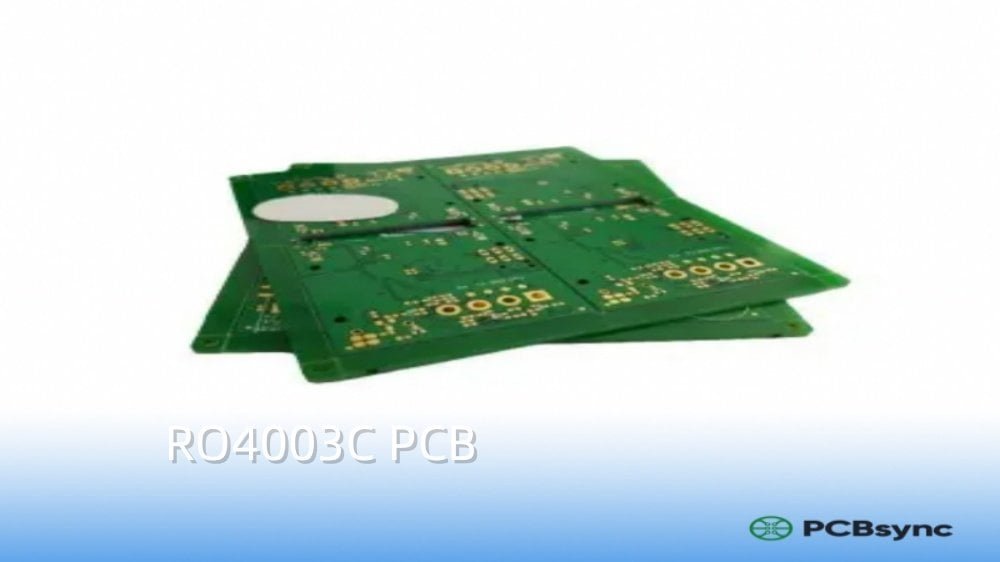
If you’re working on RF circuits, microwave systems, or anything that operates above a few GHz, you’ve probably hit the wall with standard FR4. I’ve been there—watching signal integrity fall apart as frequency climbs, dealing with inconsistent impedance, and wondering why my simulations don’t match reality. That’s when I discovered RO4003C PCB material, and honestly, it changed how I approach high-frequency design.
RO4003C is a hydrocarbon ceramic laminate from Rogers Corporation that bridges the gap between affordable FR4 and expensive PTFE materials. It delivers the electrical performance you need for serious RF work while still being manufacturable using standard PCB processes. In this guide, I’ll walk you through everything you need to know about RO4003C PCB—from material properties and specifications to practical design tips that actually work in production.
RO4003C belongs to the RO4000 series of high-frequency laminates developed by Rogers Corporation. It’s a proprietary woven glass reinforced hydrocarbon/ceramic composite that combines the electrical characteristics of PTFE-based materials with the manufacturing simplicity of standard epoxy/glass substrates.
What makes RO4003C PCB stand out is its composition. Unlike FR4 (which uses epoxy resin), RO4003C uses a thermoset hydrocarbon resin system filled with ceramic particles. This gives you low dielectric loss without the processing headaches that come with pure PTFE materials.
The material comes in two glass fabric styles—1080 and 1674—but both configurations meet identical electrical performance specifications. This consistency is crucial when you’re trying to maintain tight tolerances across different production runs.
Key Characteristics at a Glance
Hydrocarbon ceramic-filled laminate (non-PTFE)
Standard FR4 processing compatible
No special through-hole treatments required
Non-brominated (halogen-free)
Not UL 94V-0 rated (use RO4350B if you need flame rating)
RO4003C PCB Material Specifications
Before diving into design, you need to understand what you’re working with. Here’s the complete specification breakdown:
Electrical Properties
Property
Value
Test Condition
Dielectric Constant (Dk)
3.38 ± 0.05
10 GHz, Process Value
Design Dk
3.55
For circuit calculations
Dissipation Factor (Df)
0.0027
10 GHz
Loss Tangent (tanδ)
0.0021
2.5 GHz
Volume Resistivity
1.7 × 10^10 MΩ·cm
C-96/35/90
Surface Resistivity
4.2 × 10^9 MΩ
C-96/35/90
Thermal Properties
Property
Value
Notes
Glass Transition Temperature (Tg)
>280°C (>536°F)
High thermal stability
Thermal Conductivity
0.71 W/m/K
Z-axis
CTE (X-axis)
11 ppm/°C
-55 to 288°C
CTE (Y-axis)
14 ppm/°C
-55 to 288°C
CTE (Z-axis)
46 ppm/°C
-55 to 288°C
Td (Decomposition Temp)
425°C
TGA
TCDk
40 ppm/°C
-50°C to +150°C
Mechanical Properties
Property
Value
Test Method
Peel Strength
1.05 N/mm
After solder float
Flexural Strength
276 MPa
IPC-TM-650 2.4.4
Density
1.79 g/cm³
—
Moisture Absorption
0.04%
D24/23
Copper Peel
6.0 lb/in
After thermal stress
Standard Available Thicknesses
Thickness (mil)
Thickness (mm)
8
0.203
12
0.305
16
0.406
20
0.508
32
0.813
60
1.524
Standard copper weights include 0.5 oz (17μm), 1.0 oz (35μm), and 2.0 oz (70μm). Panel sizes are typically 12″×18″ (305×457mm) or 24″×18″ (610×457mm).
Why Choose RO4003C PCB Over FR4?
I get this question constantly. Here’s the honest answer: it depends on your frequency and performance requirements.
The Frequency Threshold
Below 1-2 GHz, FR4 works fine for most applications. Between 2-6 GHz, you’ll start noticing degradation with FR4. Above 6 GHz, RO4003C PCB becomes almost essential for reliable performance.
Direct Comparison: RO4003C vs FR4
Parameter
RO4003C
Standard FR4
Dielectric Constant
3.38 ± 0.05
4.2-4.8 (varies with frequency)
Loss Tangent @ 10GHz
0.0027
~0.02
Dk Stability vs Frequency
Excellent
Poor above 1 GHz
Dk Stability vs Temperature
40 ppm/°C
>200 ppm/°C
Moisture Absorption
0.04%
0.10-0.20%
Thermal Conductivity
0.71 W/m/K
0.1-0.5 W/m/K
Processing
Standard FR4 process
Standard
Cost
3-5× FR4
Baseline
The 0.0027 loss tangent versus 0.02 might not look dramatic on paper, but that’s nearly an order of magnitude difference. At 10 GHz over a 3-inch trace, you’re looking at roughly 0.5 dB additional loss with FR4 compared to RO4003C PCB. In a multi-stage RF chain, these losses compound quickly.
This is probably the most common material selection question in Rogers PCB design. Both materials are from the RO4000 series, but they serve different purposes.
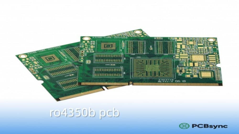
Aerospace or defense applications with strict fire safety requirements
Applications: Power amplifiers, transmitters, high-reliability systems
You cannot directly substitute RO4003C for RO4350B in an existing design without resimulating. The different Dk values will change your 50Ω microstrip line widths and affect output matching.
RO4003C PCB Applications
RO4003C PCB has become the go-to material across multiple industries. Here’s where it excels and why engineers choose it for specific use cases:
5G and Wireless Infrastructure
The rollout of 5G networks has driven massive demand for RO4003C PCB. Base station antennas, RF filters, and mmWave modules operating at 28 GHz and 39 GHz rely on this material’s low loss and stable Dk characteristics. The consistent electrical performance across temperature variations is essential for outdoor base station equipment that experiences significant thermal cycling.
Massive MIMO antenna arrays are a perfect application for RO4003C. These systems require tight phase matching between antenna elements, which demands consistent Dk across the entire panel. The material’s low loss tangent also maximizes antenna efficiency, improving overall system link budget.
Automotive Radar (ADAS)
Modern vehicles pack multiple radar sensors for adaptive cruise control, blind-spot detection, collision avoidance, and parking assistance. These 24 GHz and 77 GHz radar modules require the dimensional stability and consistent electrical properties that RO4003C delivers across temperature extremes (-40°C to +85°C operating range).
An 8×8 patch array antenna on RO4003C for 77 GHz automotive radar achieves greater than 20 dBi gain over a 1-GHz bandwidth. The material’s low TCDk ensures the antenna’s resonant frequency stays stable whether the car is parked in Arizona summer heat or Minnesota winter cold.
Aerospace and Satellite Communications
Satellite payloads, onboard processing systems, and ground station equipment use RO4003C PCB for its reliability under harsh conditions. The low moisture absorption (0.04%) is particularly valuable for equipment exposed to humidity cycling. The material’s outgassing characteristics also meet requirements for many spacecraft applications, though you should verify with Rogers for specific mission requirements.
Industrial and Test Equipment
Network analyzers, signal generators, and RF test fixtures benefit from RO4003C’s predictable characteristics. When you’re building measurement equipment, the last thing you want is your test fixture contributing uncertainty. The tight Dk tolerance (±0.05) ensures your test boards introduce minimal systematic error.
Consumer Wireless
High-end Wi-Fi 6E routers, IoT gateways, and premium wireless devices increasingly specify RO4003C for the antenna feed networks and RF front-end modules. While cost-sensitive consumer products might use FR4, flagship devices benefit from RO4003C’s improved sensitivity and range.
RO4003C PCB Design Best Practices
After years of working with this material, here are the design practices that consistently deliver good results:
Impedance Calculation and Stackup Design
Always use the design Dk value (3.55) for impedance calculations, not the process Dk (3.38). The design Dk accounts for copper surface roughness effects and real-world operating conditions.
For microstrip transmission lines on 20-mil RO4003C with 1 oz copper, a 50Ω line is approximately 45 mils wide. But don’t trust my numbers—run your own calculations using Saturn PCB Toolkit or your preferred field solver.
Typical 4-Layer Hybrid Stackup (RO4003C + FR4)
Layer
Material
Thickness
Purpose
L1
Copper
1 oz
RF signals
Core
RO4003C
20 mil
RF dielectric
L2
Copper
1 oz
Ground plane
Prepreg
FR4
8 mil
Bonding
L3
Copper
1 oz
Power/digital
Core
FR4
20 mil
Digital dielectric
L4
Copper
1 oz
Digital/ground
Hybrid stackups let you use RO4003C only where you need it (RF layers) while using cheaper FR4 for digital and power distribution layers.
Via Design Considerations
RO4003C’s low Z-axis CTE (46 ppm/°C) provides excellent plated through-hole reliability, but you should still follow good practices:
Avoid aspect ratios greater than 8:1
Use thermal relief on power plane connections
Consider via backdrilling for high-frequency signals to reduce stub resonance
For 77 GHz automotive radar, via transitions become critical—use full-wave EM simulation
Solder Mask Effects on RF Performance
Here’s something many designers overlook: solder mask affects your RF performance. Adding solder mask increases the effective Dk and dielectric losses of your microstrip and GCPW transmission lines.
For critical RF traces, consider using selective solder mask—apply it only where you need solder for component attachment, and leave the RF transmission lines exposed. Small solder mask “dams” around SMT pads have negligible effect if kept below λ/10 at your operating frequency.
Thermal Management
RO4003C’s thermal conductivity (0.71 W/m/K) is better than FR4, but thermal management still matters for power amplifiers and high-density designs:
Use thermal vias under power components
Consider copper coin inserts for high-power RF transistors
The material handles lead-free soldering temperatures (260°C) without issues
Fabrication Notes for Your Manufacturer
Include these notes in your fab drawing:
Material: Rogers RO4003C per IPC-4103/10
Dk tolerance must meet ±0.05 specification
Standard FR4 processing parameters acceptable
No special through-hole preparation required
Copper foil type: Standard ED or specify LoPro for lowest insertion loss
Impedance Control and Transmission Line Design
Getting impedance right on RO4003C PCB requires understanding a few nuances that trip up many designers.
Microstrip vs Grounded Coplanar Waveguide (GCPW)
Both transmission line structures work well on RO4003C, but they behave differently:
Microstrip is simpler to design and fabricate. For a 50Ω line on 20-mil RO4003C with 1 oz copper, you’re looking at roughly 45-mil trace width. The exact value depends on your copper surface finish and manufacturing tolerances.
GCPW (Grounded Coplanar Waveguide) offers better isolation between adjacent traces and can achieve tighter ground return paths. However, GCPW is more sensitive to manufacturing variations in the gap between signal and ground coplanar conductors.
Calculation Tips That Actually Work
When I’m doing impedance calculations for RO4003C PCB:
Start with the design Dk (3.55), not the process Dk (3.38). The design value already accounts for copper roughness effects.
Factor in copper plating thickness. After plating, your “1 oz” copper is typically 1.2-1.4 oz. This affects your final impedance.
Model at your operating frequency. RO4003C’s Dk is stable, but it does shift slightly with frequency. At 77 GHz, you might see Dk closer to 3.45.
Add manufacturing tolerance. Specify ±10% impedance tolerance for production boards. Don’t promise ±5% unless you’ve validated the capability with your fab house.
Glass Weave Effects
RO4003C uses woven glass reinforcement (1080 or 1674 styles), which creates slight Dk variations depending on whether your trace runs over glass or resin. For signals above 20 GHz or high-precision applications, consider:
Routing at 45° angles relative to the weave pattern
Using narrower traces that average over multiple weave periods
Specifying spread glass or PTFE-based materials for the most critical layers
Hybrid Stackup Design Strategies
Hybrid stackups combining RO4003C with FR4 are the sweet spot for most RF designs—you get the performance where you need it without breaking the budget.
4-Layer Hybrid Example
Here’s a proven stackup for mixed RF/digital designs:
This symmetric stackup minimizes warpage during lamination and provides RF routing on both outer layers.
Critical Rules for Hybrid Stackups
Route RF signals on cores, not prepreg. The RO4003C core has tighter Dk control than any prepreg material.
Maintain ground plane continuity. Your RF ground plane should be uninterrupted directly beneath the signal traces.
Watch for CTE mismatch. RO4003C’s CTE is similar to copper (~17 ppm/°C in-plane), which matches well with FR4. But verify with your fab house that they’ve successfully processed similar hybrid stackups.
Use compatible bondply materials. Rogers RO4450B or RO4450F prepregs bond well to RO4003C cores. Standard FR4 prepreg also works but may introduce slight Dk discontinuities.
Manufacturing and Processing Guidelines
One of RO4003C PCB’s biggest advantages is its compatibility with standard FR4 fabrication processes. Here’s what your manufacturer needs to know:
Drilling Parameters
Parameter
Recommendation
Surface Speed
<500 SFM
Chip Load
>0.002″ (0.05mm)
Stack Height
<70% of flute length
Entry Material
Standard aluminum or phenolic
Lamination
RO4003C laminates at standard FR4 temperatures and pressures. For hybrid stackups, use RO4450B or RO4450F bondply materials from Rogers.
Copper Foil Options
Standard electrodeposited (ED) copper: Works for most applications
LoPro (reverse treated foil): Reduces insertion loss by improving copper-dielectric interface smoothness. The LoPro resin adds approximately 0.7 mil (18μm) per core.
Lead Attachment
Standard soldering processes work without modification. No plasma treatment or sodium etch required (unlike PTFE materials).
Common RO4003C PCB Design Mistakes to Avoid
After reviewing hundreds of RO4003C designs, I see the same mistakes repeatedly. Here’s what to watch out for:
Mistake 1: Using Process Dk Instead of Design Dk
The datasheet lists Dk as 3.38 ± 0.05, but that’s the process Dk measured under specific conditions. For impedance calculations, use 3.55 (the design Dk). Using 3.38 will result in traces that are too narrow and impedances that run high.
Mistake 2: Ignoring Copper Surface Roughness
Standard electrodeposited copper has a rough surface that increases effective Dk and insertion loss, especially above 10 GHz. For frequencies beyond 20 GHz, specify LoPro (reverse treated) foil. The smoother copper-dielectric interface can reduce insertion loss by 10-15% at 40 GHz.
Mistake 3: Placing RF Traces on Prepreg Layers
In multilayer boards, always route RF signals on the laminate core, not over prepreg. Prepreg has looser Dk tolerances and can introduce inconsistencies in your transmission line impedance.
Mistake 4: Neglecting Via Transitions
At mmWave frequencies, the inductance of a simple through-via can destroy your match. For 77 GHz automotive radar designs, ground vias surrounding the signal via are essential. Full-wave EM simulation of via transitions is not optional at these frequencies.
Mistake 5: Over-Specifying Tolerances
Requesting ±3% impedance tolerance on RO4003C PCB drives up cost significantly. Most applications work fine with ±10%, which is standard capability. Only tighten tolerances when your design sensitivity analysis truly requires it.
Mistake 6: Forgetting About Assembly Impacts
The low dielectric loss that makes RO4003C great for RF also means it’s more transparent to IR reflow ovens. Monitor your thermal profile carefully—the board may heat differently than FR4 during assembly.
Testing and Validation of RO4003C PCB Designs
Once your boards arrive, proper validation ensures they meet specifications.
Impedance Verification
Request TDR (Time Domain Reflectometry) coupons from your manufacturer. Compare measured impedance to your design target. Typical acceptance criteria is ±10%, but verify your specific requirements.
Insertion Loss Measurement
For critical RF traces, measure S21 insertion loss versus frequency using a VNA (Vector Network Analyzer). Compare to your simulation predictions. RO4003C should show loss of approximately 0.02-0.03 dB/inch at 10 GHz for 50Ω microstrip.
Return Loss Verification
Measure S11 to verify impedance matching. Well-designed 50Ω lines on RO4003C should achieve better than 20 dB return loss across your operating band.
Environmental Testing
For automotive and aerospace applications, validate performance across temperature (-40°C to +85°C or wider). RO4003C’s low TCDk ensures minimal impedance shift, but always verify on your actual hardware.
Cost Optimization Strategies
RO4003C isn’t cheap—expect to pay 3-5× the cost of FR4. Here’s how to manage costs:
Use Hybrid Stackups
Route RF signals on RO4003C layers, keep digital and power on FR4. A 6-layer hybrid board is often more cost-effective than a 4-layer all-RO4003C board.
Right-Size Your Material Selection
Don’t specify RO4003C for a 900 MHz IoT application where FR4 would work fine. Reserve premium materials for frequencies and performance requirements that actually demand them.
Panel Utilization
RO4003C comes in standard panel sizes. Work with your manufacturer to maximize panel utilization and minimize waste.
Volume Discounts
For production quantities, negotiate directly with Rogers-authorized distributors. Lead times are typically 4-6 weeks, so plan ahead.
Useful Resources and Downloads
Here are official resources for RO4003C PCB design:
Official Documentation
RO4003C Datasheet (PDF): Available from Rogers Corporation website at rogerscorp.com
RO4000 Series Fabrication Guide: Detailed processing parameters from Rogers
IPC-4103/10 Specification: Industry standard for RO4003C compliance
Design Tools
Rogers MWI Calculator: Free online microwave impedance calculator at rogerscorp.com
Polar Instruments SI9000: Professional impedance calculation software
Technical Support
Rogers Technology Support Hub: Technical papers and application notes
Rogers Design Support: Contact Rogers for complex stackup guidance
Frequently Asked Questions About RO4003C PCB
Is RO4003C PCB suitable for frequencies above 40 GHz?
Yes, RO4003C maintains stable performance up to 77 GHz and beyond, which is why it’s widely used in automotive radar applications. However, at mmWave frequencies, copper surface roughness becomes increasingly important. Consider specifying LoPro foil for frequencies above 40 GHz to minimize conductor losses.
Can I mix RO4003C with FR4 in a multilayer PCB?
Absolutely. Hybrid stackups combining RO4003C and FR4 are common and cost-effective. Use RO4003C for your RF signal layers and FR4 for digital and power layers. Rogers RO4450B prepreg works well for bonding dissimilar materials. Just ensure your RF signals route on the RO4003C cores, not on prepreg layers.
Why doesn’t RO4003C have a UL 94V-0 flame rating?
RO4003C is non-brominated (halogen-free), which is why it doesn’t achieve the UL 94V-0 rating. If your application requires flame rating certification, use RO4350B instead. For many commercial and industrial applications, the flame rating isn’t required, making RO4003C’s halogen-free construction an environmental advantage.
What’s the maximum operating temperature for RO4003C PCB?
With a Tg above 280°C and decomposition temperature of 425°C, RO4003C handles all standard PCB assembly processes including lead-free soldering. For continuous operation, the material performs reliably across the typical electronics temperature range of -55°C to +125°C. The low TCDk (40 ppm/°C) ensures your electrical performance remains stable across this range.
How does moisture affect RO4003C PCB performance?
RO4003C’s moisture absorption is extremely low at 0.04%—significantly better than FR4’s typical 0.10-0.20%. This means your dielectric constant and loss tangent remain stable even in humid environments. For outdoor equipment, satellite systems, and marine electronics, this stability is a significant advantage over other laminate materials.
Conclusion
RO4003C PCB material has earned its place as the workhorse of high-frequency circuit design. It delivers the electrical performance needed for demanding RF and microwave applications while remaining compatible with standard PCB manufacturing processes. Whether you’re designing 5G antennas, automotive radar modules, or satellite communication equipment, understanding RO4003C’s properties and design requirements will help you build boards that work the first time.
The key takeaways: use the design Dk (3.55) for impedance calculations, leverage hybrid stackups to optimize cost, pay attention to solder mask effects on RF traces, and work with a manufacturer experienced in Rogers materials. With these fundamentals in place, RO4003C PCB gives you the foundation for successful high-frequency designs.
Inquire: Call 0086-755-23203480, or reach out via the form below/your sales contact to discuss our design, manufacturing, and assembly capabilities.
Quote: Email your PCB files to Sales@pcbsync.com (Preferred for large files) or submit online. We will contact you promptly. Please ensure your email is correct.
Notes: For PCB fabrication, we require PCB design file in Gerber RS-274X format (most preferred), *.PCB/DDB (Protel, inform your program version) format or *.BRD (Eagle) format. For PCB assembly, we require PCB design file in above mentioned format, drilling file and BOM. Click to download BOM template To avoid file missing, please include all files into one folder and compress it into .zip or .rar format.


