Inquire: Call 0086-755-23203480, or reach out via the form below/your sales contact to discuss our design, manufacturing, and assembly capabilities.
Quote: Email your PCB files to Sales@pcbsync.com (Preferred for large files) or submit online. We will contact you promptly. Please ensure your email is correct.
Notes: For PCB fabrication, we require PCB design file in Gerber RS-274X format (most preferred), *.PCB/DDB (Protel, inform your program version) format or *.BRD (Eagle) format. For PCB assembly, we require PCB design file in above mentioned format, drilling file and BOM. Click to download BOM template To avoid file missing, please include all files into one folder and compress it into .zip or .rar format.
RF PCB Design: The Complete Guide to Materials, Layout & Best Practices
Looking to master RF PCB design? This comprehensive guide covers everything from material selection and impedance matching to layout techniques that actually work. Whether you’re building your first radio frequency board or troubleshooting signal integrity issues, you’ll find practical solutions here.
What Makes RF PCB Design Different?
If you’ve ever worked with standard PCBs and then jumped into RF design, you know the frustration. What worked perfectly fine at lower frequencies suddenly falls apart when you push into the MHz and GHz range. That’s because RF PCB design plays by a completely different set of rules.
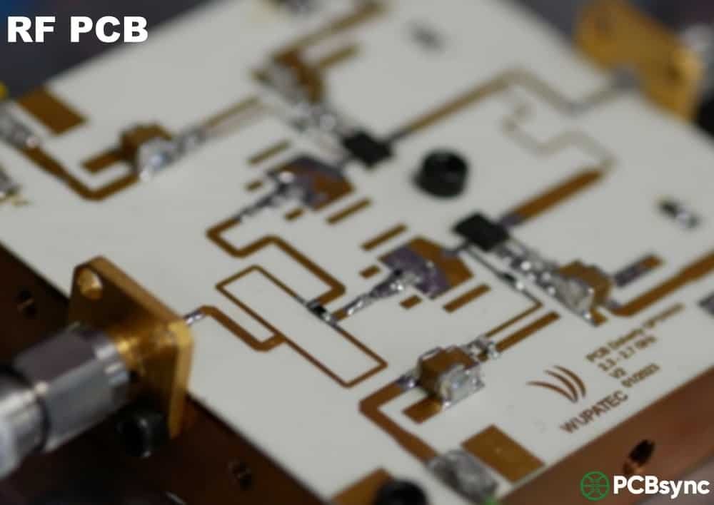
An RF PCB (radio frequency printed circuit board) operates at frequencies above 100 MHz. Once you cross that threshold, every trace, via, and ground connection starts behaving like a transmission line. Signals don’t just flow through copper anymore—they radiate, reflect, and interfere with each other in ways that can kill your design.
The wavelength of a 1 GHz signal is about 30 centimeters in free space—shorter in a PCB substrate. When trace lengths approach a significant fraction of the wavelength, the distributed nature of the circuit becomes impossible to ignore. Parasitic inductance and capacitance that you could safely neglect at 10 MHz suddenly dominate circuit behavior.
The good news? Once you understand the core principles, RF PCB design becomes much more predictable. This guide breaks down the essential factors: materials, impedance control, stack-up design, grounding strategies, and common mistakes that trip up even experienced engineers.
The demand for high-frequency circuit boards has exploded over the past decade. 5G networks operate at millimeter-wave frequencies up to 77 GHz. Automotive radar systems need precise signal control for collision detection and autonomous driving features. IoT devices pack wireless communication into tiny form factors that challenge even experienced designers.
Poor RF design doesn’t just cause minor performance issues—it causes complete system failures. A mismatched impedance can reflect half your signal power back to the source. Bad grounding creates noise that drowns out weak RF signals. The wrong substrate material adds insertion losses that make receivers deaf to legitimate signals.
Consider what happens when an automotive radar fails. The vehicle might not detect an obstacle in time, potentially causing an accident. Medical devices that use RF communication need absolute reliability. Satellite links that cost millions to deploy can’t tolerate design errors. The stakes in RF PCB design have never been higher.
RF PCB Design Suite | PCBSync Engineering Tools
📡
RF PCB Design Suite
PCBSync Engineering Tools
RF PCB Design Suite
Comprehensive engineering tools for high-frequency PCB design. Calculate impedance, compare materials, estimate costs, and optimize your RF designs.
85+
RF Materials
6
Calculators
77 GHz
Max Frequency
⚡
Impedance Calculator
Microstrip, Stripline, CPWG
Calculate transmission line impedance for various geometries with RF substrate materials.
📊
Materials Database
85+ RF Substrates
Compare Rogers, Taconic, Arlon, Isola, and more with detailed electrical properties.
💰
Cost Estimator
Instant Quotes
Get estimated manufacturing costs based on material, layers, and specifications.
Rogers 4350B
Dk 3.48
Df 0.0037 @ 10GHz
Megtron 6
Dk 3.4
Df 0.002 @ 10GHz
Taconic RF-35
Dk 3.5
Df 0.0018 @ 10GHz
Isola Astra MT77
Dk 3.0
Df 0.0017 @ 10GHz
💡 Quick Tip
For frequencies above 10 GHz, consider materials with Df < 0.003 to minimize signal loss. Rogers RO3003 and Taconic TLY-5 are excellent choices for mmWave applications.
• For 50Ω microstrip: W ≈ 2×H for εr ≈ 4
• Keep W/H between 0.5 and 4 for accurate models
• Consider via spacing for ground return path
• Edge coupling increases with narrower spacing
⚡
Stripline Impedance Calculator
Centered trace between ground planes
mm
mm
mm
Characteristic Impedance
—Ω
Propagation Delay
—
W/B Ratio
—
📋
Stripline Benefits
When to use stripline
✅ Advantages
• Better shielding (enclosed by ground planes)
• Lower radiation loss
• Less susceptible to EMI
• Consistent impedance
⚠️ Considerations
• More complex fabrication
• Requires via transitions
• Higher insertion loss than microstrip
• Component placement on surface only
• Gap (G) ≥ 2× trace thickness
• Keep G < H for good ground coupling
• W/(W+2G) ≈ 0.5 for 50Ω typical
🔗 Via Stitching
• Space vias < λ/10 apart
• Place vias close to gap edge
• Use multiple via rows for mmWave
✅ CPWG Advantages
• Easy component mounting (same plane)
• Good for flip-chip/wire bonding
• Lower dispersion than microstrip
• Excellent for mmWave (>20 GHz)
🌊
Wavelength Calculator
Free-space and guided wavelength
Free-Space λ₀
—
Guided λg
—
λ/4 (Stub)
—
λ/2
—
📊
Common RF Bands
Quick reference wavelengths
Band
Frequency
λ₀ (mm)
Application
L-Band
1-2 GHz
150-300
GPS, Mobile
S-Band
2-4 GHz
75-150
Wi-Fi, Radar
C-Band
4-8 GHz
37.5-75
5G, Satellite
X-Band
8-12 GHz
25-37.5
Radar, Space
Ku-Band
12-18 GHz
16.7-25
Satellite TV
K-Band
18-27 GHz
11-16.7
5G mmWave
Ka-Band
27-40 GHz
7.5-11
5G, Satcom
V-Band
40-75 GHz
4-7.5
WiGig, Radar
W-Band
75-110 GHz
2.7-4
Auto Radar
📏
Skin Depth Calculator
Current penetration depth in conductors
Skin Depth (δ)
—μm
3δ Depth (99%)
—
Min Cu Thickness
—
💡 Design Rule
Copper thickness should be ≥ 3× skin depth for full current utilization. At high frequencies, current flows mainly on conductor surface.
📊
Skin Depth Reference
Copper skin depth at various frequencies
Frequency
Skin Depth (Cu)
Recommended Cu
1 MHz
66 μm
2 oz (70 μm)
10 MHz
21 μm
1 oz (35 μm)
100 MHz
6.6 μm
0.5 oz (18 μm)
1 GHz
2.1 μm
0.5 oz (18 μm)
5 GHz
0.93 μm
0.25 oz (9 μm)
10 GHz
0.66 μm
0.25 oz (9 μm)
28 GHz
0.39 μm
0.25 oz (9 μm)
77 GHz
0.24 μm
0.25 oz (9 μm)
📉
Transmission Line Loss
Conductor + Dielectric losses
GHz
mm
Dielectric Loss
—
Conductor Loss (est)
—
Total Loss
—
Loss per inch
—
📊
Material Loss Comparison
Insertion loss @ 10 GHz, 1 inch
Material
Df @10GHz
Loss (dB/in)
Rating
RT/duroid 5880
0.0009
0.10
★★★★★
RO3003
0.0013
0.15
★★★★★
Taconic TLY-5
0.0009
0.10
★★★★★
Megtron 6
0.002
0.22
★★★★
RO4003C
0.0027
0.30
★★★★
RO4350B
0.0037
0.40
★★★
Isola I-Tera MT40
0.0031
0.35
★★★
FR-4
0.020
2.2
★
📚
Stack-Up Builder
Configure your PCB layers
📋
Stack-Up Preview
4-Layer RF/Digital Hybrid
Layer
Type
Material
Thickness
L1
Signal (RF)
RO4350B
35 μm Cu
–
Prepreg
RO4450F
0.1 mm
L2
Ground
–
35 μm Cu
–
Core
FR-4
1.0 mm
L3
Power
–
35 μm Cu
–
Prepreg
FR-4 PP
0.2 mm
L4
Signal
–
35 μm Cu
💡 RF Stack-Up Tips
• Place RF traces on outer layers adjacent to ground
• Use continuous ground plane under RF routing
• Consider thermal relief for RF components
• Match Dk between prepreg and core for hybrid stacks
📐
Common RF Stack-Ups
Industry-standard configurations
2-Layer Simple RF
RO4350B
Signal-Ground, 10-20 mil core. Best for simple RF circuits, filters, antennas.
RF PCB Material Selection: Getting the Foundation Right
Material choice makes or breaks RF PCB performance. You can't compensate for a bad substrate with clever routing—the physics just won't cooperate. The substrate determines signal propagation speed, loss characteristics, and thermal behavior. Here's what you need to know about picking the right material for your application.
Dielectric Constant (Dk): Why It Matters
The dielectric constant determines how fast signals travel through your board and directly affects trace impedance. Lower Dk values (typically below 4) allow faster signal propagation and narrower traces for the same impedance. This matters because narrower traces mean denser routing and potentially smaller boards.
Here's the catch that trips up many designers: Dk isn't constant. It changes with frequency, temperature, and even the direction of measurement in materials with woven glass reinforcement. FR4's dielectric constant can drift by 10% or more as frequency increases, causing unpredictable impedance variations across your board. At 1 GHz, your carefully calculated 50-ohm trace might measure 45 or 55 ohms depending on where you probe it.
For serious RF work above 1 GHz, you need materials with stable Dk values. Rogers laminates maintain their dielectric properties within 2% across a wide frequency range, which is why they dominate high-frequency applications. This consistency lets you trust your impedance calculations and predict circuit behavior accurately.
Dissipation Factor (Df): The Signal Killer
Dissipation factor measures how much signal energy gets converted to heat as it travels through the substrate. Think of it as the "lossyness" of your material. Every inch of trace on a high-loss material weakens your signal.
Standard FR4 has a Df around 0.02, meaning 2% of your signal power disappears with every wavelength of travel. That might sound small, but at 10 GHz with long traces, you're losing substantial signal strength. Rogers materials typically offer Df values between 0.001 and 0.004—roughly 5-20 times better than FR4. For a receiver trying to detect weak signals, this difference determines whether the system works or fails.
The loss equation gets worse at higher frequencies. Dielectric loss increases roughly proportionally with frequency, while conductor loss (from the skin effect) increases with the square root of frequency. Both effects combine to make long traces at high frequencies especially problematic.
Don't assume you always need expensive RF materials. For applications below 1 GHz with short trace lengths, standard FR4 often works fine. Many WiFi designs at 2.4 GHz use high-quality FR4 successfully—if you keep traces short and control your impedance carefully.
The breaking point typically comes around 3-5 GHz or with long RF signal paths. That's when FR4's inconsistent Dk and high losses become impossible to ignore. If you're designing anything for 5G millimeter-wave, automotive radar at 77 GHz, or satellite applications, budget for Rogers or PTFE materials from the start. The cost of a board respin far exceeds the material premium.
Hybrid stack-ups offer a middle ground. You can use Rogers material for critical RF layers while using cheaper FR4 for power and digital signal layers. This approach balances performance with cost, though it adds manufacturing complexity and requires careful attention to thermal expansion mismatches between materials.
Impedance Matching: The Heart of RF PCB Design
Impedance matching isn't optional in RF design—it's fundamental. When impedances don't match between your source, transmission line, and load, signals bounce back toward the source instead of reaching their destination. These reflections waste power and can damage sensitive components like power amplifiers.
Understanding Characteristic Impedance
Every trace on an RF PCB has a characteristic impedance (Z0) determined by its width, thickness, distance from the ground plane, and the substrate's dielectric constant. The industry has standardized on two values: 50Ω for most RF applications and 75Ω for video and cable systems.
Why 50Ω? It's a compromise between power handling (better at lower impedances around 30Ω) and loss (lower at higher impedances around 77Ω). The 50-ohm standard hits a sweet spot that works well for most applications. Plus, most RF components—filters, amplifiers, antennas, connectors—are designed around 50Ω, which simplifies matching throughout your signal chain.
The maximum power transfer theorem tells us that power delivery is maximized when source and load impedances match. Any mismatch creates reflections described by the reflection coefficient. A 2:1 VSWR (voltage standing wave ratio) means about 11% of your power reflects back. At 3:1 VSWR, you lose 25%. Poor matches don't just waste power—they can create standing waves that damage transmitter output stages.
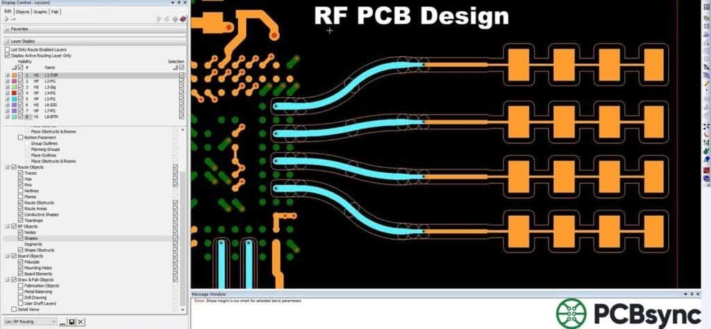
Transmission Line Types for RF PCBs
RF PCBs use three main transmission line structures, each with different characteristics and trade-offs:
Microstrip: The trace sits on the outer layer with a ground plane beneath it. This is the simplest and most common structure for RF routing. It's easy to manufacture and allows for component placement directly on the trace. However, microstrips radiate some energy and are susceptible to external interference. The fields extend both above and below the trace, with the air above having a different dielectric constant than the substrate below.
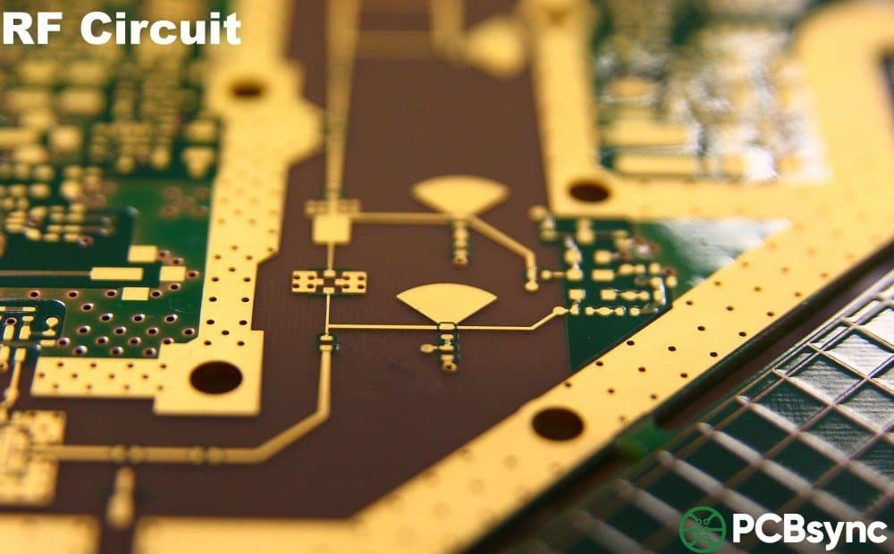
Stripline: The trace is sandwiched between two ground planes on inner layers. Striplines offer better isolation and essentially zero radiation, making them ideal for sensitive receive paths and situations where crosstalk must be minimized. The trade-off is that you can't place components directly on stripline traces, and routing becomes more constrained.
Coplanar Waveguide (CPW): Ground copper runs alongside the signal trace on the same layer, sometimes with an additional ground plane below (CPWG). CPW provides excellent isolation between adjacent traces and works well for very high frequencies where microstrip becomes problematic. The trade-off is more complex impedance calculations, tighter manufacturing tolerances, and sensitivity to gap dimensions.
Practical Impedance Control Tips
Get your stack-up from the fabricator first. They know their process tolerances, and impedance calculations depend on exact dielectric thicknesses. A 10% error in assumed thickness means a 5% error in impedance.
Use impedance calculators religiously. Don't guess trace widths. Software tools or online calculators should determine every RF trace dimension based on your actual stack-up.
Maintain consistent trace width throughout. Any width change creates an impedance discontinuity that reflects signals. If you must change width, use a tapered transition.
Request tighter tolerances for critical paths. Standard PCB manufacturing holds ±10% impedance. For critical RF paths, ask for ±5% or better—most quality manufacturers can achieve this.
Match component pad sizes to trace width. Pads that are significantly wider than traces create capacitive discontinuities. Design your land patterns with impedance in mind.
RF PCB Stack-Up Design Strategies
The layer stack-up determines how well your RF PCB controls impedance, shields sensitive signals, and manages return currents. Even simple RF boards typically need at least four layers to work properly. Trying to squeeze RF functionality onto a two-layer board usually ends in frustration.
Basic 4-Layer RF Stack-Up
The standard 4-layer RF stack-up provides a solid foundation:
Layer 1 (Top): RF components and signal traces on RF-grade material
Layer 2: Solid ground plane (critical for impedance control and return paths)
Layer 3: Power plane with appropriate decoupling
Layer 4 (Bottom): Digital components and non-RF signals
This arrangement keeps RF signals immediately adjacent to their ground reference, ensuring controlled impedance and short return paths. Digital noise on the bottom layer stays isolated from sensitive RF circuits. The ground plane between RF and digital sections acts as a shield.
Advanced 6-Layer and 8-Layer Stack-Ups
More complex designs often require six or eight layers. A typical 6-layer RF stack-up might use: Top (RF signals), Ground, Signal/Power, Ground, Signal, Bottom (digital). This provides stripline routing options for sensitive signals that need maximum isolation. The additional layers also allow better separation between power domains.
Eight-layer boards become necessary when you have multiple RF sections that need isolation from each other, or when the digital section is complex enough to require its own dedicated signal layers. The key principle remains the same: every signal layer should have an adjacent, unbroken ground reference plane.
Stack-Up Rules That Save Projects
Never route RF signals over split planes. If your ground plane has a gap, return currents have to detour around it, creating a loop antenna that radiates and picks up interference. This single mistake has killed countless RF designs.
Keep dielectric thickness consistent. Variable spacing between signal and ground layers means variable impedance. Work with your fabricator to understand their lamination tolerances.
Don't route signals between power and ground planes. The return current path becomes unpredictable, coupling through the power plane capacitance. You'll get EMI problems that are difficult to diagnose.
Consider CTE matching in hybrid stackups. When combining different materials like Rogers and FR4, thermal expansion mismatches can cause warping or delamination. Discuss this with your fabricator before finalizing the design.
Grounding Strategies for RF PCBs
Good grounding separates working RF designs from paperweights. At high frequencies, ground isn't just a reference voltage—it's an active part of your signal path. The return current must have a low-impedance path immediately beneath the signal trace.
The Ground Plane: Your Best Friend
A solid, uninterrupted ground plane directly beneath your RF signals provides a low-impedance return path and helps contain electromagnetic fields. Breaks in the ground plane force return currents to find alternate routes, creating loops that radiate energy. Even small gaps can cause significant problems at GHz frequencies.
Some designers still split ground planes between analog and digital sections, thinking this prevents digital noise from contaminating analog circuits. In RF design, this approach usually causes more problems than it solves. The split forces return currents across the gap, creating exactly the kind of common-impedance coupling you were trying to prevent. A single, continuous ground plane with careful component placement works better than trying to isolate ground regions.
Via Stitching: More Is Better
Via stitching connects ground areas on different layers and creates a low-inductance path for return currents. For RF boards, add stitching vias liberally:
Along both sides of RF traces (forms a coplanar waveguide effect and improves isolation)
Around the board perimeter (blocks edge radiation and improves EMC performance)
Under shielding cans and RF components (provides low-inductance grounding)
Between isolated ground areas if you must have any plane splits
Space stitching vias no more than λ/20 apart at your highest frequency of operation. At 10 GHz (λ = 30mm), that means vias every 1.5mm or closer. This sounds like a lot of vias, and it is. RF boards often have more vias for grounding than for signals.
Decoupling Capacitor Placement
Decoupling capacitors must be placed as close as possible to IC power pins—ideally on the same layer to minimize via inductance. Use multiple capacitor values in parallel to cover different frequency ranges. A typical arrangement might include 10µF for low frequencies, 100nF for mid-range, and 100pF or smaller for high-frequency bypassing.
Each decoupling capacitor needs its own ground via. Sharing vias between capacitors increases effective inductance and reduces bypassing effectiveness at high frequencies. The inductance of even a short trace or shared via can negate the benefit of the capacitor at GHz frequencies.
RF PCB Layout Best Practices
Layout decisions can make or break your RF design. Component placement, trace routing, and separation between RF and digital sections all affect performance in ways that can be difficult to predict without experience.
Component Placement Guidelines
Group RF components together to minimize trace lengths and keep the RF section compact. Shorter traces mean lower loss and less opportunity for interference.
Keep digital ICs at least 10-20mm away from sensitive RF components. More distance is always better. Clock oscillators and switching regulators are particularly noisy.
Place decoupling capacitors as close as possible to IC power pins. On the same layer is best. If you must use vias, keep them short.
Position antennas at board edges away from other components, ground pours, and metal enclosures that could detune them.
Orient connectors for straight RF signal paths to avoid unnecessary bends. Every bend is a potential impedance discontinuity.
Consider the signal flow and place components in a logical sequence that minimizes crossing traces and backtracking.
Trace Routing Rules
RF traces aren't like digital traces. Every bend, via, and width change affects signal integrity in measurable ways.
Use 45° angles or smooth curves instead of 90° corners. Sharp corners create impedance bumps, radiate energy, and can reflect signals.
Minimize vias on RF signal paths. Each via adds inductance (typically 0.5-1nH) and creates a discontinuity. If you must use vias, add ground vias nearby to provide a return path.
Keep RF traces as short as possible. Longer traces mean more loss, more delay, and more opportunity for interference. Plan your layout to minimize RF path lengths.
Maintain adequate spacing between traces. Parallel RF traces should be at least 3x the trace width apart to minimize crosstalk. More spacing is better.
Don't run RF and digital signals in parallel. If they must cross, do it at 90° to minimize coupling. Long parallel runs couple significant energy between traces.
Watch out for stubs. Any unterminated trace segment acts as a stub that can cause resonances. This includes unused pads on components and test points.
Common RF PCB Design Mistakes to Avoid
Learning from others' mistakes saves time, money, and frustration. Here are the errors that regularly destroy RF designs—and how to avoid them:
Mistake 1: Ignoring Return Current Paths
Every signal needs a return path. At high frequencies, return currents flow directly beneath the signal trace, not through the nearest ground connection. This is physics, not a guideline. Route over a solid ground plane, and you're fine. Route over a split or missing ground plane, and your return current creates a radiating loop. This is probably the single most common cause of RF design failures.
Mistake 2: Using FR4 Where It Doesn't Belong
Budget constraints push designers toward FR4, but using it for 5+ GHz designs or long RF traces guarantees poor performance. Calculate your expected insertion loss before committing to a material. If the math shows excessive loss, upgrade your substrate. The material cost difference is trivial compared to a board respin.
Mistake 3: Inconsistent Impedance Throughout the Signal Path
Changing trace widths, adding sharp bends, or using oversized pads creates impedance discontinuities. These cause reflections that degrade signal quality and can create standing waves. Maintain consistent geometry throughout your RF signal path. If you must change impedance, use proper matching networks.
Mistake 4: Skipping Electromagnetic Simulation
RF problems are hard to debug on fabricated boards because you can't see electromagnetic fields. Simulation catches impedance mismatches, crosstalk issues, and radiation problems before you spend money on prototypes. Tools like Ansys HFSS, Keysight ADS, or even free options like openEMS can prevent expensive respins. The time invested in simulation pays back many times over.
Mistake 5: Poor Thermal Management
Power amplifiers and other active RF components generate significant heat. Temperature changes affect dielectric properties and can shift impedance, degrading performance. Hot spots can also cause reliability problems. Include thermal vias, copper pours connected to ground, and heat sinks in your design from the start.
Mistake 6: Inadequate EMI Shielding
RF circuits both generate and are susceptible to electromagnetic interference. Sensitive receive sections need shielding from digital circuits and power supplies. High-power transmit sections can interfere with nearby circuits. Use metal shields, ground-stitched via fences, and proper enclosure design to contain and block interference.
Testing and Validating Your RF PCB Design
Even well-designed RF boards need verification. Testing catches manufacturing defects, validates simulation results, and verifies that your design performs as intended in the real world.
Essential RF Test Equipment
Vector Network Analyzer (VNA): Measures S-parameters, impedance, return loss, and insertion loss. Essential for any RF work. Modern VNAs cover DC to 50+ GHz.
Spectrum Analyzer: Shows frequency content, spurious emissions, harmonic distortion, and interference. Critical for compliance testing.
Time Domain Reflectometer (TDR): Locates impedance discontinuities along traces. Shows exactly where problems occur, not just that they exist.
Near-field probe set: Finds locations of electromagnetic radiation on the board. Invaluable for EMI debugging.
Signal generator: Provides clean test signals for receiver sensitivity measurements and characterization.
Key Performance Measurements
Focus your testing on these critical parameters:
Return loss (S11): Should be below -10 dB for acceptable matching, below -15 dB for good performance, below -20 dB for excellent matching.
Insertion loss (S21): Compare measured results to your calculated loss budget. Excessive loss indicates material problems, impedance mismatches, or manufacturing defects.
VSWR: Voltage Standing Wave Ratio should be below 2:1 for most applications, ideally below 1.5:1 for critical paths.
Isolation between channels: Verify that adjacent channels or traces don't couple significantly. Typical requirements are 20-40 dB isolation.
Phase consistency: For phased arrays and other phase-sensitive applications, verify phase matching between channels.
Putting It All Together
RF PCB design demands attention to details that simply don't matter in low-frequency work. Material selection, impedance control, stack-up planning, and careful grounding all contribute to success. Skip any of these, and you'll spend time debugging problems that could have been prevented with proper upfront planning.
Start with your requirements: operating frequency, acceptable loss, environmental conditions, and budget. Choose materials that meet your electrical needs without excessive cost. Plan your stack-up with solid ground planes adjacent to RF signals. Control impedance throughout every signal path. Keep digital noise away from sensitive RF sections.
Simulate before you fabricate. Modern electromagnetic simulation tools can predict performance with remarkable accuracy when given correct inputs. Test thoroughly when boards arrive—don't assume everything works just because power comes up. Document what works so you can repeat it on future projects.
RF PCB design has a reputation for being difficult, even mystical. But it's really just physics and engineering discipline. Understand the principles, follow established guidelines, verify your results, and iterate based on measurements. With practice, RF design becomes predictable rather than mysterious.
Frequently Asked Questions About RF PCB Design
What frequency makes a PCB an "RF PCB"?
The industry generally considers any board operating above 100 MHz an RF PCB. At this frequency, traces start behaving as transmission lines rather than simple conductors, and distributed effects become significant. Boards operating above 2 GHz are often called microwave PCBs, though the underlying principles remain the same. The distinction matters because higher frequencies require progressively more attention to material selection, impedance control, and layout practices. At 10 GHz and above, even tiny geometrical details affect circuit behavior.
Can I use FR4 for RF PCB applications?
FR4 works for some RF applications, particularly below 1 GHz with short trace lengths. Many WiFi designs at 2.4 GHz use high-quality FR4 variants successfully when engineers keep traces short and maintain tight impedance control. However, FR4's inconsistent dielectric constant and high loss tangent make it unsuitable for frequencies above 3-5 GHz or any application requiring predictable, repeatable performance. For serious RF work—5G millimeter-wave, automotive radar at 77 GHz, or satellite applications—invest in Rogers, PTFE, or other low-loss materials from the start.
Why is 50Ω the standard impedance for RF systems?
The 50Ω standard represents a practical engineering compromise discovered in the early days of coaxial cable development. Lower impedance (around 30Ω) provides maximum power handling capability, while higher impedance (around 77Ω) minimizes signal loss. Engineers chose 50Ω because it balances both characteristics reasonably well for most applications. Additionally, decades of 50Ω standardization mean most RF components—connectors, cables, amplifiers, filters, and test equipment—are designed for 50Ω systems. Using a standard value eliminates matching networks between stages and simplifies system design significantly.
How many layers do I need for an RF PCB?
Most RF designs require at least four layers: a top signal layer, a ground plane, a power plane, and a bottom signal layer. The critical requirement is having a solid, unbroken ground plane immediately adjacent to your RF signals for impedance control and return current flow. Two-layer boards can work for very simple RF circuits if you dedicate most of the bottom layer to ground and keep RF traces short. Complex designs with mixed RF and digital circuitry often need six or more layers to properly separate and shield different functional sections. Eight-layer boards become necessary when you have multiple RF sections requiring isolation from each other.
What's the biggest mistake beginners make in RF PCB design?
The most common and damaging mistake is ignoring return current paths. Every RF signal needs a low-impedance return path immediately beneath it—this is physics, not a suggestion. At high frequencies, return currents don't find the nearest ground connection; they flow directly under the signal trace. When designers route RF traces over split ground planes, gaps, or areas with no ground at all, return currents must find alternate routes, creating loop antennas that radiate energy and pick up interference. This single mistake is responsible for more failed RF designs than any other factor. Always maintain solid, continuous ground beneath RF traces, and use via stitching to connect ground areas on different layers.
Inquire: Call 0086-755-23203480, or reach out via the form below/your sales contact to discuss our design, manufacturing, and assembly capabilities.
Quote: Email your PCB files to Sales@pcbsync.com (Preferred for large files) or submit online. We will contact you promptly. Please ensure your email is correct.
Notes: For PCB fabrication, we require PCB design file in Gerber RS-274X format (most preferred), *.PCB/DDB (Protel, inform your program version) format or *.BRD (Eagle) format. For PCB assembly, we require PCB design file in above mentioned format, drilling file and BOM. Click to download BOM template To avoid file missing, please include all files into one folder and compress it into .zip or .rar format.


