Inquire: Call 0086-755-23203480, or reach out via the form below/your sales contact to discuss our design, manufacturing, and assembly capabilities.
Quote: Email your PCB files to Sales@pcbsync.com (Preferred for large files) or submit online. We will contact you promptly. Please ensure your email is correct.
Notes: For PCB fabrication, we require PCB design file in Gerber RS-274X format (most preferred), *.PCB/DDB (Protel, inform your program version) format or *.BRD (Eagle) format. For PCB assembly, we require PCB design file in above mentioned format, drilling file and BOM. Click to download BOM template To avoid file missing, please include all files into one folder and compress it into .zip or .rar format.
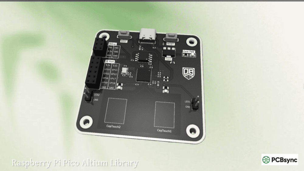
Raspberry Pi Pico Altium Library: RP2040 Schematic & PCB Footprint
The Raspberry Pi Pico changed everything when it launched in 2021. For the first time, Raspberry Pi released a microcontroller board instead of a full Linux computer, and the engineering community responded enthusiastically. Now, designers want to integrate the Pico—or the RP2040 chip directly—into custom PCBs. The challenge? Finding a reliable Raspberry Pi Pico Altium Library with accurate schematics and footprints.
I’ve designed several RP2040-based boards and learned that library quality makes or breaks a project. An incorrect footprint means boards that don’t work, wasted money on fabrication, and delayed schedules. This guide covers where to download verified libraries, how to use them correctly, and essential PCB design considerations for successful RP2040 projects.
Before downloading any Raspberry Pi Pico Altium Library, you need to understand the different components available. You can either design around the Pico board itself (using it as a module) or design with the bare RP2040 chip.
Pico Board Variants
Raspberry Pi offers several Pico variants, each with different features:
Board
Chip
Wireless
Flash
Dimensions
Key Feature
Pico
RP2040
None
2MB
21 x 51mm
Original board
Pico H
RP2040
None
2MB
21 x 51mm
Pre-soldered headers
Pico W
RP2040
WiFi/BT
2MB
21 x 51mm
CYW43439 wireless
Pico WH
RP2040
WiFi/BT
2MB
21 x 51mm
Wireless + headers
Pico 2
RP2350
None
4MB
21 x 51mm
Upgraded processor
Pico 2 W
RP2350
WiFi/BT
4MB
21 x 51mm
RP2350 + wireless
The Pico boards feature castellated holes along both edges, allowing them to be soldered directly to carrier boards as surface-mount modules. This makes them incredibly versatile for production designs.
RP2040 Chip Specifications
For designs using the bare RP2040 chip, here are the critical specifications:
Specification
Value
CPU
Dual-core ARM Cortex-M0+
Max Clock Speed
133 MHz
SRAM
264 KB
On-chip Flash
None (external required)
GPIO
30 (26 exposed on Pico)
ADC
4-channel 12-bit, 500 ksps
PWM
16 channels
Package
QFN-56 (7mm × 7mm)
Operating Voltage
1.8V – 3.3V I/O
The RP2040’s unique feature is its Programmable I/O (PIO) system—two PIO blocks with four state machines each that can implement custom protocols in hardware.
Where to Download Raspberry Pi Pico Altium Libraries
Finding accurate libraries is the first step toward a successful design. Here are the most reliable sources.
SnapEDA (SnapMagic Search)
SnapEDA provides free, verified libraries for both the Pico board and RP2040 chip.
Available Components:
Raspberry Pi Pico (board footprint)
Raspberry Pi Pico W (wireless variant)
RP2040 (bare chip)
RP2040-PICO-PC (third-party variants)
Download Process:
Visit snapeda.com and search “Raspberry Pi Pico” or “RP2040”
Select your component from the results
Choose “Altium” as the export format
Download the .zip file
Extract the .SchLib and .PcbLib files
Import into your Altium project
SnapEDA footprints follow IPC-7351B standards and include 3D models for mechanical verification.
Ultra Librarian
Ultra Librarian offers manufacturer-verified CAD models with detailed 3D STEP files:
Features:
Free download after registration
Includes accurate 3D models
Available in 22+ CAD formats including Altium
Verified against manufacturer datasheets
The RP2040 library from Ultra Librarian includes the proper QFN-56 footprint with exposed thermal pad specifications matching Raspberry Pi’s datasheet.
SamacSys (Component Search Engine)
SamacSys provides the Pico library through their Library Loader plugin:
Installation:
Download Library Loader from componentsearchengine.com
Install and configure for Altium Designer
Search for “PICO” or “RP2040”
Click “Add to Design” to import directly
The plugin adds components directly to your project without manual file management.
GitHub Community Libraries
Several community repositories offer tested Altium libraries:
Repository
Contents
Notes
amgsus/RPi-Pico-Altium
Pico board symbol & footprint
Includes castellated pad footprint
Various RP2040 projects
Complete project files
Reference designs with libraries
Downloading from GitHub:
Navigate to the repository
Click “Code” → “Download ZIP”
Extract and locate .SchLib and .PcbLib files
Add to your Altium project
Raspberry Pi Official Resources
Raspberry Pi provides official KiCad design files that can be imported into Altium:
Hardware Design Guide with RP2040
Pico board reference design files
RP2040 minimal design example
While these are in KiCad format, Altium’s import wizard can convert them successfully.
How to Import Pico Libraries into Altium Designer
Proper library installation ensures components work correctly across all your projects.
Installing Schematic and PCB Libraries
For separate .SchLib and .PcbLib files:
Open Altium Designer
Go to the Components panel
Click the menu icon and select File-based Libraries Preferences
In the Installed tab, click Install
Browse to and select your .SchLib file
Repeat for the .PcbLib file
Click Close
The libraries now appear in your Components panel for all projects.
Adding Libraries to a Specific Project
For project-specific use:
Right-click your project in the Projects panel
Select Add Existing to Project
Navigate to your library files
Select both .SchLib and .PcbLib files
The libraries appear under your project structure
Verifying Library Accuracy
After importing, always verify your libraries:
Open the Components panel
Search for “Pico” or “RP2040”
Preview the schematic symbol
Check the footprint tab
For the Pico board, verify 40 pins in two rows of 20
For RP2040, verify QFN-56 footprint with 56 pads plus thermal pad
Print the footprint at 1:1 scale and compare against actual hardware before ordering boards.
RP2040 Hardware Design Essentials
When designing with the bare RP2040 chip rather than the Pico module, several critical design considerations apply.
Required External Components
The RP2040 requires external components that don’t exist on-chip:
Component
Purpose
Typical Value/Part
QSPI Flash
Program storage
W25Q128JVS (16MB max)
Crystal
System clock
12 MHz, 30ppm
Load Capacitors
Crystal circuit
Per crystal datasheet
Decoupling Caps
Power filtering
0.1µF per IOVDD/DVDD
3.3V Regulator
Power supply
XC6206, AP2112K
1.1V Core
Internal LDO output
Internal to RP2040
Power Supply Design
The RP2040 has specific power requirements:
IOVDD (I/O Power): 1.8V to 3.3V, supplies GPIO and peripherals. Use 0.1µF decoupling on each IOVDD pin.
DVDD (Digital Core): 1.1V nominal, generated by internal LDO from VREG_VIN. Add 1µF capacitor on VREG_VOUT.
USB_VDD: Power for USB PHY, requires 3.3V with 0.1µF decoupling.
ADC_AVDD: Analog power for ADC, filter from 3.3V for best performance.
For battery-powered applications, consider that the RP2040 typically draws 20-50mA depending on clock speed and peripheral usage.
QSPI Flash Layout Guidelines
The external flash is critical—poor layout causes boot failures:
Trace Length: Keep QSPI traces under 20mm total length.
Trace Width: Minimum 0.15mm (6 mil) recommended.
Matching: Match trace lengths for CLK, D0, D1, D2, D3, and CS signals.
Ground Plane: Maintain solid ground under all QSPI traces.
Flash Selection: Stick with Winbond W25Q series for guaranteed compatibility. Other manufacturers may have incompatible command sets.
Crystal Oscillator Layout
The 12 MHz crystal requires careful placement:
Place crystal and load capacitors as close to RP2040 as possible
Keep crystal traces short and away from high-speed signals
Route XIN and XOUT traces on top layer only
Avoid running other traces near crystal signals
Use guard ground around crystal if space permits
USB Design Considerations
The RP2040 includes a USB 1.1 PHY (Full-Speed 12 Mbps):
Series Resistors: Add 27Ω resistors on D+ and D- lines near the RP2040.
Impedance: Target 90Ω differential impedance for USB traces.
Trace Length: Keep traces short; USB 1.1 is forgiving but matching still helps.
ESD Protection: Add TVS diode protection at the USB connector.
Should I use the Pico board or the bare RP2040 chip?
For prototyping and low-volume production, the Pico board is usually the better choice. It includes all necessary external components (flash, crystal, power regulation) and is already tested. The castellated holes allow SMD mounting on carrier boards. Use the bare RP2040 chip when you need custom flash sizes, specific power regulation, smaller footprint, or very high volume production where component cost matters.
What flash chip should I use with the RP2040?
Stick with the Winbond W25Q series—specifically W25Q16, W25Q32, W25Q64, or W25Q128 (up to 16MB maximum). These are explicitly supported and tested by Raspberry Pi. Other flash chips may use incompatible command sets that prevent proper boot. I learned this the hard way when a Macronix chip didn’t work despite having similar specifications. The savings from alternative chips aren’t worth the risk.
Can I hand-solder the RP2040 QFN-56 package?
The QFN-56 package is extremely challenging to hand-solder due to the small 0.4mm pitch and exposed thermal pad. You’ll need either a hot air rework station (set to ~275°C) or a reflow oven. The exposed pad requires solder paste and proper thermal vias. For prototyping, I recommend using the Pico module instead—it solves all these assembly challenges and costs only a few dollars more than sourcing individual components.
Why does my RP2040 design not boot?
Common boot failure causes include: QSPI flash not compatible (use W25Q series), incorrect crystal frequency (must be 12 MHz), missing or incorrect decoupling capacitors, TESTEN pin not tied to ground, flash chip not properly soldered or connected, or BOOTSEL circuit interference. The RP2040’s built-in USB bootloader means a completely blank chip should still enumerate over USB when BOOTSEL is held during power-up. If it doesn’t, the problem is hardware.
How do I program the RP2040 on my custom board?
There are two methods: USB bootloader (hold BOOTSEL, connect USB, drag-and-drop UF2 file) or SWD debugging interface (requires SWCLK and SWDIO connections plus a debug probe like the Raspberry Pi Debug Probe or J-Link). For production, include test points for SWD and ensure the BOOTSEL button or jumper is accessible. Most custom boards include both methods for flexibility during development and testing.
Building Your First RP2040 Design
With a proper Raspberry Pi Pico Altium Library in hand and understanding of the design requirements, you’re ready to create your own RP2040-based PCB. Start with Raspberry Pi’s minimal design example as a reference, verify your library footprints against the datasheets, and pay careful attention to the QSPI flash and crystal layout.
The RP2040 platform offers exceptional value—a powerful dual-core processor with rich peripherals at a remarkably low cost. Whether you’re using the Pico module on a carrier board or designing with the bare chip, proper library selection and hardware design practices will ensure your project succeeds.
Remember that Raspberry Pi’s hardware design guide is your primary reference. It contains detailed layout recommendations, component selection guidance, and verified design examples that represent years of engineering experience. When in doubt, follow their recommendations—they’ve tested these designs extensively.
Your custom RP2040 board awaits. Get the right libraries, follow the guidelines, and start designing.
Inquire: Call 0086-755-23203480, or reach out via the form below/your sales contact to discuss our design, manufacturing, and assembly capabilities.
Quote: Email your PCB files to Sales@pcbsync.com (Preferred for large files) or submit online. We will contact you promptly. Please ensure your email is correct.
Notes: For PCB fabrication, we require PCB design file in Gerber RS-274X format (most preferred), *.PCB/DDB (Protel, inform your program version) format or *.BRD (Eagle) format. For PCB assembly, we require PCB design file in above mentioned format, drilling file and BOM. Click to download BOM template To avoid file missing, please include all files into one folder and compress it into .zip or .rar format.


