Inquire: Call 0086-755-23203480, or reach out via the form below/your sales contact to discuss our design, manufacturing, and assembly capabilities.
Quote: Email your PCB files to Sales@pcbsync.com (Preferred for large files) or submit online. We will contact you promptly. Please ensure your email is correct.
Notes: For PCB fabrication, we require PCB design file in Gerber RS-274X format (most preferred), *.PCB/DDB (Protel, inform your program version) format or *.BRD (Eagle) format. For PCB assembly, we require PCB design file in above mentioned format, drilling file and BOM. Click to download BOM template To avoid file missing, please include all files into one folder and compress it into .zip or .rar format.
In this guide, I’ll walk you through everything you need to know about radar PCB design, from choosing the right substrate materials to avoiding common pitfalls that can ruin your signal integrity. Whether you’re designing a 24GHz industrial sensor or a 77GHz automotive radar module, the principles we’ll cover here will help you build boards that actually work.
A radar PCB is a specialized printed circuit board designed to handle the transmission, reception, and processing of high-frequency electromagnetic signals used in radar systems. Unlike standard PCBs that operate at relatively low frequencies, radar PCBs work with signals ranging from 1 GHz all the way up to 77 GHz or higher.
The fundamental job of a radar PCB is straightforward: send out a radio wave, wait for it to bounce off something, and analyze the return signal. But at microwave and millimeter-wave frequencies, every trace becomes a transmission line, every via introduces inductance, and every material choice affects your loss budget. That’s why radar PCB design demands a level of precision that most other PCB types simply don’t require.
How Radar Systems Work
Before diving into design specifics, let’s quickly review how radar actually works. A radar system transmits electromagnetic pulses through an antenna. When these pulses hit an object, they bounce back to the receiver. By measuring the time delay between transmission and reception, the system calculates distance. By analyzing frequency shifts (Doppler effect), it determines velocity.
The radar PCB connects and supports all the key components that make this happen:
Transmitter: Amplifies the signal for transmission
Receiver: Captures and processes return signals
Antenna: Often integrated directly onto the PCB as patch arrays
Signal Processor: Extracts range, velocity, and angle information
Duplexer: Switches between transmit and receive modes
Types of Radar PCB Systems
Different radar applications require different PCB architectures. Here’s a breakdown of the main types you’ll encounter:
Doppler Radar PCB
Doppler radar PCBs detect motion by measuring frequency shifts in returned signals. When a target moves toward the radar, the return frequency increases; when it moves away, the frequency decreases. These boards are commonly used in motion sensors, speed detectors, and traffic monitoring systems.
FMCW Radar PCB
Frequency-Modulated Continuous Wave (FMCW) radar represents the most common architecture in modern automotive and industrial applications. The system transmits a signal that continuously sweeps across a frequency range — typically 76-77 GHz for long-range automotive radar or 77-81 GHz for short-range applications.
By comparing the transmitted chirp with the received signal, FMCW radar can simultaneously determine distance and velocity. This makes it ideal for Advanced Driver Assistance Systems (ADAS), where knowing both how far away a car is and how fast it’s approaching matters critically.
Pulsed Radar PCB
Pulsed radar sends high-power bursts of energy and measures the time until echoes return. This architecture excels at long-range detection and is commonly used in air traffic control, weather monitoring, and military surveillance systems. The radar PCB must handle high instantaneous power levels while maintaining precise timing.
Phased Array Radar PCB
Phased array radar PCBs represent the cutting edge of radar technology. Instead of mechanically rotating an antenna, these systems use arrays of antenna elements with individually controlled phase shifters. By adjusting the phase of each element, the beam can be steered electronically in microseconds.
The PCB design challenges for phased arrays are immense: you need extremely tight phase and length matching across all transmission lines, sophisticated thermal management for power amplifiers, and careful isolation between hundreds or thousands of elements.
MIMO Radar PCB
Multiple-Input Multiple-Output (MIMO) radar uses multiple transmit and receive antennas to create a virtual array with improved angular resolution. This architecture is increasingly common in automotive radar, where space constraints limit physical antenna size but high resolution remains essential.
Radar PCB Materials: Making the Right Choice
Material selection is arguably the most critical decision in radar PCB design. At high frequencies, standard FR-4 simply doesn’t cut it — the dielectric losses become unacceptable, and the dielectric constant varies too much with temperature and frequency.
Why Standard FR-4 Falls Short
FR-4 works fine for digital circuits and even RF designs below about 1-2 GHz. But as frequency increases, several problems emerge: high loss tangent (around 0.02) causes significant signal attenuation; the dielectric constant varies with frequency and temperature; and the material absorbs moisture, changing electrical characteristics.
High-Frequency Materials for Radar PCB
For serious radar work, you need materials specifically engineered for high-frequency performance:
PTFE (Polytetrafluoroethylene) substrates offer the lowest dielectric losses available. Ceramic-filled PTFE laminates like RO3003 provide the stable dielectric constant and ultra-low loss required for 77 GHz millimeter-wave designs. The downside? PTFE is more challenging to process — it requires specialized drilling and plating techniques.
Hybrid Stackups
Many radar PCB designs use hybrid stackups that combine high-frequency materials only where needed. For example, you might use RO3003 for the top two layers containing the antenna and RF front-end, then transition to lower-cost FR-4 for the digital processing layers below. This approach optimizes both performance and cost.
Radar PCB Design Guidelines
Getting the design right requires attention to dozens of details. Here are the key considerations every radar PCB designer should understand:
Impedance Control
At radar frequencies, every trace is a transmission line. Maintaining consistent 50Ω impedance throughout your RF signal path is absolutely critical. Any impedance discontinuity creates reflections that degrade performance and can cause interference.
Layer Stackup Design
A well-designed layer stackup provides controlled impedance, good isolation between RF and digital sections, and robust ground planes. The key principle: keep RF signals on dedicated layers with uninterrupted ground planes directly beneath them.
Radar PCBs use several transmission line topologies:
Microstrip: The trace sits on top of the PCB with a ground plane below. Easy to manufacture and good for antenna connections.
Stripline: The trace is sandwiched between two ground planes. Better shielded and preferred for sensitive receiver paths.
Coplanar Waveguide (CPW): Ground planes run alongside the signal trace on the same layer. Useful for MMIC transitions.
Via Design for High Frequency
Standard through-hole vias introduce significant inductance at radar frequencies. At 77 GHz, a via stub of just 0.5mm can create enough reflection to seriously degrade your signal. Key via techniques include:
Blind and buried vias: Shorter via stubs mean less parasitic inductance
Back-drilling: Remove unused via stubs after plating to eliminate resonant structures
Via fencing: Rows of ground vias surrounding RF traces prevent mode conversion and crosstalk
Laser-drilled microvias: Smaller diameter vias with lower inductance for high-density designs
Antenna Integration
Many modern radar PCBs integrate the antenna directly onto the board as patch antenna arrays. The patch dimensions must be accurate to fractions of a millimeter because resonant frequency depends directly on physical size. At 77 GHz, even 50-micron variation can shift center frequency enough to affect performance.
Thermal Management
Radar systems often include power amplifiers (PAs) that generate significant heat. Power amplifier efficiency at millimeter-wave frequencies is typically only 20-30%, meaning 70-80% of input power becomes heat. Your thermal design should include:
Thermal vias: Dense arrays under hot components conduct heat to internal ground planes
Metal core substrates: Aluminum or copper cores for extreme power densities
Heatsink mounting: Direct attachment provisions with proper thermal interface materials
Copper pours: Large areas connected to ground spread heat across the board
Radar PCB technology has moved far beyond military origins into countless civilian applications:
Automotive Radar PCB
The automotive industry has become the largest consumer of radar PCBs. ADAS systems rely on 77 GHz radar PCBs for automatic emergency braking, lane change assistance, parking assist, and autonomous driving sensor fusion.
Radar Type
Frequency
Range
Application
Long-Range (LRR)
76-77 GHz
10-250m
Adaptive cruise control
Short-Range (SRR)
77-81 GHz
0.2-30m
Blind spot detection
Corner Radar
77 GHz
0.1-80m
Cross-traffic alert
Industrial and Commercial Radar PCB
Beyond automotive, radar PCBs enable level measurement for tanks, motion detection for security systems, traffic monitoring, robotics collision avoidance, and healthcare applications like contactless vital sign monitoring.
Aerospace and Defense Radar PCB
Military and aerospace applications demand the highest performance and reliability. These include airborne radar, ship-based navigation, missile guidance, and satellite-based synthetic aperture radar (SAR) systems.
Common Radar PCB Design Challenges
Signal Integrity at mmWave Frequencies
At 77 GHz, the wavelength on a typical PCB substrate is about 2.3mm. This means features that seem trivially small at lower frequencies become significant. Solutions include using 3D electromagnetic simulation, minimizing RF trace lengths, and validating with TDR measurements.
EMI/EMC Compliance
Radar systems must meet strict electromagnetic compatibility requirements. Best practices include comprehensive RF shielding, careful ground plane design, filtered power supplies, and proper cable shield grounding.
Manufacturing Yield
High-frequency PCBs are sensitive to manufacturing variations including Dk tolerance, copper roughness, etching variations, and layer registration errors. Work closely with fabricators and build margin into your design.
Cost Optimization
High-frequency materials cost significantly more than FR-4 — PTFE laminates can cost 20-50 times more. Strategies include hybrid stackups, standard panel sizes, design for test, and volume planning for material pricing.
Testing and Quality Assurance for Radar PCB
A radar PCB isn’t done when it leaves fabrication — rigorous testing ensures it meets performance requirements:
Network analyzer measurements: S-parameters verify impedance matching and insertion loss
Isola Group: https://www.isola-group.com/ — RF materials including Astra MT77
Taconic: https://www.taconic.com/ — RF-35 and high-frequency laminates
Design Software and Tools
Altium Designer: Industry-standard PCB design with RF features
Cadence AWR Microwave Office: RF/microwave circuit simulation
Ansys HFSS: 3D electromagnetic field simulation
Keysight ADS: Signal integrity and RF design
Standards and Specifications
IPC-2221: Generic standard for PCB design
IPC-2252: Design standard for RF/microwave PCBs
IPC-6018: High-frequency PCB qualification
Frequently Asked Questions About Radar PCB
What frequency range do radar PCBs typically operate at?
Radar PCBs operate across a wide spectrum. Industrial sensors often use 24 GHz, while automotive ADAS systems use 76-81 GHz (commonly called 77 GHz radar). Military systems may operate from 1 GHz to over 100 GHz. Any PCB operating above 1 GHz generally requires specialized high-frequency design techniques.
Why can’t I use standard FR-4 for radar PCB designs?
Standard FR-4 has a high loss tangent (around 0.02) causing unacceptable signal attenuation at radar frequencies. Its dielectric constant also varies with frequency and temperature, making precise impedance control impossible. For frequencies above 1-2 GHz, you need specialized materials like Rogers RO3003 or PTFE-based laminates with loss tangents below 0.004.
How does 77 GHz automotive radar PCB differ from lower frequency designs?
At 77 GHz, the wavelength is approximately 2.3mm, making every detail critical. Key differences include: mandatory ultra-low-loss materials, smooth copper foils for reduced loss, much tighter manufacturing tolerances, integrated antenna elements, and more challenging thermal management due to smaller component sizes.
What is the typical cost difference between radar PCB and standard PCB?
Radar PCBs typically cost 3-10 times more than equivalent-complexity standard PCBs. Cost increases come from expensive high-frequency materials (PTFE can cost 10-20x more than FR-4), tighter manufacturing tolerances, lower yields, and additional testing requirements. Hybrid stackups using expensive materials only in RF layers help control costs.
How do I choose between microstrip and stripline for radar PCB routing?
Choose microstrip for easy component access, antenna feeds, and simpler manufacturing. Choose stripline for better isolation from external interference, sensitive receiver paths, and minimizing crosstalk. Many radar PCB designs use both: microstrip for outer layer antenna connections and stripline for internal RF routing where shielding matters.
Conclusion
Designing radar PCBs is challenging but incredibly rewarding work. The technology enables everything from keeping drivers safe on highways to monitoring weather patterns that affect millions of people. Getting it right requires understanding high-frequency electromagnetic behavior, selecting appropriate materials, following rigorous design practices, and validating through simulation and testing.
Whether you’re new to radar PCB design or looking to refine your skills, focus on the fundamentals: proper impedance control, clean ground planes, appropriate material selection, and attention to every detail that affects signal integrity. Master these basics, and you’ll be well-equipped to tackle even the most demanding radar applications.
The field continues advancing rapidly, with higher frequencies, greater integration, and new applications emerging constantly. Stay curious, keep learning, and don’t hesitate to reach out to material suppliers and fabricators for guidance — they’ve seen countless designs and can offer valuable insights specific to your application.
If you’ve ever worked on high-frequency circuit design, you know that radar PCB isn’t just another board — it’s one of the most demanding projects an engineer can tackle. I’ve spent years working with RF and microwave circuits, and I can tell you that getting a radar PCB right requires understanding everything from material science to electromagnetic theory.
In this guide, I’ll walk you through everything you need to know about radar PCB design, from choosing the right substrate materials to avoiding common pitfalls that can ruin your signal integrity. Whether you’re designing a 24GHz industrial sensor or a 77GHz automotive radar module, the principles we’ll cover here will help you build boards that actually work.
What is a Radar PCB?
A radar PCB is a specialized printed circuit board designed to handle the transmission, reception, and processing of high-frequency electromagnetic signals used in radar systems. Unlike standard PCBs that operate at relatively low frequencies, radar PCBs work with signals ranging from 1 GHz all the way up to 77 GHz or higher.
The fundamental job of a radar PCB is straightforward: send out a radio wave, wait for it to bounce off something, and analyze the return signal. But at microwave and millimeter-wave frequencies, every trace becomes a transmission line, every via introduces inductance, and every material choice affects your loss budget. That’s why radar PCB design demands a level of precision that most other PCB types simply don’t require.
How Radar Systems Work
Before diving into design specifics, let’s quickly review how radar actually works. A radar system transmits electromagnetic pulses through an antenna. When these pulses hit an object, they bounce back to the receiver. By measuring the time delay between transmission and reception, the system calculates distance. By analyzing frequency shifts (Doppler effect), it determines velocity.
The radar PCB connects and supports all the key components that make this happen:
Transmitter: Amplifies the signal for transmission
Receiver: Captures and processes return signals
Antenna: Often integrated directly onto the PCB as patch arrays
Signal Processor: Extracts range, velocity, and angle information
Duplexer: Switches between transmit and receive modes
Types of Radar PCB Systems
Different radar applications require different PCB architectures. Here’s a breakdown of the main types you’ll encounter:
Doppler Radar PCB
Doppler radar PCBs detect motion by measuring frequency shifts in returned signals. When a target moves toward the radar, the return frequency increases; when it moves away, the frequency decreases. These boards are commonly used in motion sensors, speed detectors, and traffic monitoring systems.
FMCW Radar PCB
Frequency-Modulated Continuous Wave (FMCW) radar represents the most common architecture in modern automotive and industrial applications. The system transmits a signal that continuously sweeps across a frequency range — typically 76-77 GHz for long-range automotive radar or 77-81 GHz for short-range applications.
By comparing the transmitted chirp with the received signal, FMCW radar can simultaneously determine distance and velocity. This makes it ideal for Advanced Driver Assistance Systems (ADAS), where knowing both how far away a car is and how fast it’s approaching matters critically.
Pulsed Radar PCB
Pulsed radar sends high-power bursts of energy and measures the time until echoes return. This architecture excels at long-range detection and is commonly used in air traffic control, weather monitoring, and military surveillance systems. The radar PCB must handle high instantaneous power levels while maintaining precise timing.
Phased Array Radar PCB
Phased array radar PCBs represent the cutting edge of radar technology. Instead of mechanically rotating an antenna, these systems use arrays of antenna elements with individually controlled phase shifters. By adjusting the phase of each element, the beam can be steered electronically in microseconds.
The PCB design challenges for phased arrays are immense: you need extremely tight phase and length matching across all transmission lines, sophisticated thermal management for power amplifiers, and careful isolation between hundreds or thousands of elements.
MIMO Radar PCB
Multiple-Input Multiple-Output (MIMO) radar uses multiple transmit and receive antennas to create a virtual array with improved angular resolution. This architecture is increasingly common in automotive radar, where space constraints limit physical antenna size but high resolution remains essential.
Radar PCB Materials: Making the Right Choice
Material selection is arguably the most critical decision in radar PCB design. At high frequencies, standard FR-4 simply doesn’t cut it — the dielectric losses become unacceptable, and the dielectric constant varies too much with temperature and frequency.
Why Standard FR-4 Falls Short
FR-4 works fine for digital circuits and even RF designs below about 1-2 GHz. But as frequency increases, several problems emerge: high loss tangent (around 0.02) causes significant signal attenuation; the dielectric constant varies with frequency and temperature; and the material absorbs moisture, changing electrical characteristics.
High-Frequency Materials for Radar PCB
For serious radar work, you need materials specifically engineered for high-frequency performance:
Material
Dk
Df
Best Application
Rogers RO3003
3.00
0.0013
77GHz automotive radar
Rogers RO4350B
3.48
0.0037
Mid-range, cost-sensitive
Rogers RO4835
3.48
0.0031
77GHz, oxidation resistant
Isola Astra MT77
3.00
0.0017
Automotive, wide temp
Shengyi mmWave77
3.00
0.0010
Ultra-low loss ADAS
PTFE/Teflon
2.1-2.5
0.0009
Highest performance
PTFE-Based Materials
PTFE (Polytetrafluoroethylene) substrates offer the lowest dielectric losses available. Ceramic-filled PTFE laminates like RO3003 provide the stable dielectric constant and ultra-low loss required for 77 GHz millimeter-wave designs. The downside? PTFE is more challenging to process — it requires specialized drilling and plating techniques.
Hybrid Stackups
Many radar PCB designs use hybrid stackups that combine high-frequency materials only where needed. For example, you might use RO3003 for the top two layers containing the antenna and RF front-end, then transition to lower-cost FR-4 for the digital processing layers below. This approach optimizes both performance and cost.
Radar PCB Design Guidelines
Getting the design right requires attention to dozens of details. Here are the key considerations every radar PCB designer should understand:
Impedance Control
At radar frequencies, every trace is a transmission line. Maintaining consistent 50Ω impedance throughout your RF signal path is absolutely critical. Any impedance discontinuity creates reflections that degrade performance and can cause interference.
Layer Stackup Design
A well-designed layer stackup provides controlled impedance, good isolation between RF and digital sections, and robust ground planes. The key principle: keep RF signals on dedicated layers with uninterrupted ground planes directly beneath them.
Layer
Function
Material
L1
RF/Antenna
RO3003
L2
Ground
Copper
L3
RF routing
RO3003
L4
Ground
Copper
L5
Digital/Control
FR-4
L6
Power/Ground
FR-4
Transmission Line Structures
Radar PCBs use several transmission line topologies:
Microstrip: The trace sits on top of the PCB with a ground plane below. Easy to manufacture and good for antenna connections.
Stripline: The trace is sandwiched between two ground planes. Better shielded and preferred for sensitive receiver paths.
Coplanar Waveguide (CPW): Ground planes run alongside the signal trace on the same layer. Useful for MMIC transitions.
Via Design for High Frequency
Standard through-hole vias introduce significant inductance at radar frequencies. At 77 GHz, a via stub of just 0.5mm can create enough reflection to seriously degrade your signal. Key via techniques include:
Blind and buried vias: Shorter via stubs mean less parasitic inductance
Back-drilling: Remove unused via stubs after plating to eliminate resonant structures
Via fencing: Rows of ground vias surrounding RF traces prevent mode conversion and crosstalk
Laser-drilled microvias: Smaller diameter vias with lower inductance for high-density designs
Antenna Integration
Many modern radar PCBs integrate the antenna directly onto the board as patch antenna arrays. The patch dimensions must be accurate to fractions of a millimeter because resonant frequency depends directly on physical size. At 77 GHz, even 50-micron variation can shift center frequency enough to affect performance.
Thermal Management
Radar systems often include power amplifiers (PAs) that generate significant heat. Power amplifier efficiency at millimeter-wave frequencies is typically only 20-30%, meaning 70-80% of input power becomes heat. Your thermal design should include:
Thermal vias: Dense arrays under hot components conduct heat to internal ground planes
Metal core substrates: Aluminum or copper cores for extreme power densities
Heatsink mounting: Direct attachment provisions with proper thermal interface materials
Copper pours: Large areas connected to ground spread heat across the board
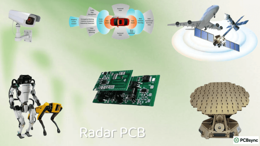
Radar PCB Applications Across Industries
Radar PCB technology has moved far beyond military origins into countless civilian applications:
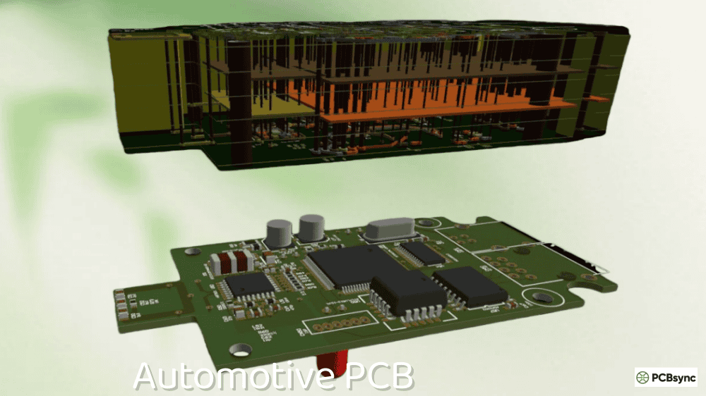
Automotive Radar PCB
The automotive industry has become the largest consumer of radar PCBs. ADAS systems rely on 77 GHz radar PCBs for automatic emergency braking, lane change assistance, parking assist, and autonomous driving sensor fusion.
Radar Type
Frequency
Range
Application
Long-Range (LRR)
76-77 GHz
10-250m
Adaptive cruise control
Short-Range (SRR)
77-81 GHz
0.2-30m
Blind spot detection
Corner Radar
77 GHz
0.1-80m
Cross-traffic alert
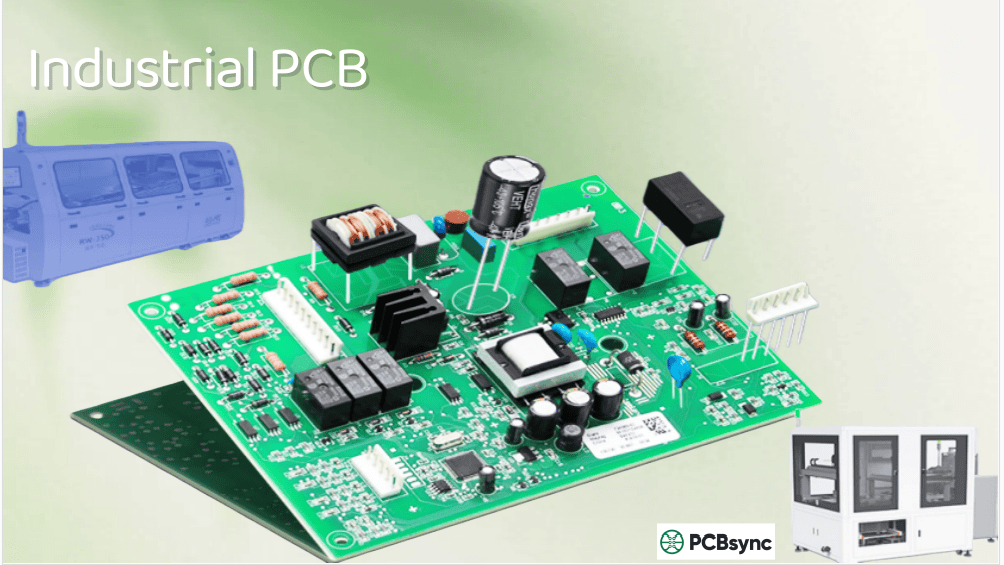
Industrial and Commercial Radar PCB
Beyond automotive, radar PCBs enable level measurement for tanks, motion detection for security systems, traffic monitoring, robotics collision avoidance, and healthcare applications like contactless vital sign monitoring.
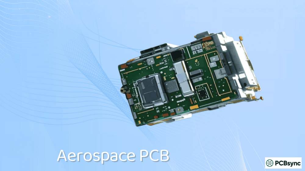
Aerospace and Defense Radar PCB
Military and aerospace applications demand the highest performance and reliability. These include airborne radar, ship-based navigation, missile guidance, and satellite-based synthetic aperture radar (SAR) systems.
Common Radar PCB Design Challenges
Signal Integrity at mmWave Frequencies
At 77 GHz, the wavelength on a typical PCB substrate is about 2.3mm. This means features that seem trivially small at lower frequencies become significant. Solutions include using 3D electromagnetic simulation, minimizing RF trace lengths, and validating with TDR measurements.
EMI/EMC Compliance
Radar systems must meet strict electromagnetic compatibility requirements. Best practices include comprehensive RF shielding, careful ground plane design, filtered power supplies, and proper cable shield grounding.
Manufacturing Yield
High-frequency PCBs are sensitive to manufacturing variations including Dk tolerance, copper roughness, etching variations, and layer registration errors. Work closely with fabricators and build margin into your design.
Cost Optimization
High-frequency materials cost significantly more than FR-4 — PTFE laminates can cost 20-50 times more. Strategies include hybrid stackups, standard panel sizes, design for test, and volume planning for material pricing.
Testing and Quality Assurance for Radar PCB
A radar PCB isn’t done when it leaves fabrication — rigorous testing ensures it meets performance requirements:
Network analyzer measurements: S-parameters verify impedance matching and insertion loss
Isola Group: https://www.isola-group.com/ — RF materials including Astra MT77
Taconic: https://www.taconic.com/ — RF-35 and high-frequency laminates
Design Software and Tools
Altium Designer: Industry-standard PCB design with RF features
Cadence AWR Microwave Office: RF/microwave circuit simulation
Ansys HFSS: 3D electromagnetic field simulation
Keysight ADS: Signal integrity and RF design
Standards and Specifications
IPC-2221: Generic standard for PCB design
IPC-2252: Design standard for RF/microwave PCBs
IPC-6018: High-frequency PCB qualification
Frequently Asked Questions About Radar PCB
What frequency range do radar PCBs typically operate at?
Radar PCBs operate across a wide spectrum. Industrial sensors often use 24 GHz, while automotive ADAS systems use 76-81 GHz (commonly called 77 GHz radar). Military systems may operate from 1 GHz to over 100 GHz. Any PCB operating above 1 GHz generally requires specialized high-frequency design techniques.
Why can’t I use standard FR-4 for radar PCB designs?
Standard FR-4 has a high loss tangent (around 0.02) causing unacceptable signal attenuation at radar frequencies. Its dielectric constant also varies with frequency and temperature, making precise impedance control impossible. For frequencies above 1-2 GHz, you need specialized materials like Rogers RO3003 or PTFE-based laminates with loss tangents below 0.004.
How does 77 GHz automotive radar PCB differ from lower frequency designs?
At 77 GHz, the wavelength is approximately 2.3mm, making every detail critical. Key differences include: mandatory ultra-low-loss materials, smooth copper foils for reduced loss, much tighter manufacturing tolerances, integrated antenna elements, and more challenging thermal management due to smaller component sizes.
What is the typical cost difference between radar PCB and standard PCB?
Radar PCBs typically cost 3-10 times more than equivalent-complexity standard PCBs. Cost increases come from expensive high-frequency materials (PTFE can cost 10-20x more than FR-4), tighter manufacturing tolerances, lower yields, and additional testing requirements. Hybrid stackups using expensive materials only in RF layers help control costs.
How do I choose between microstrip and stripline for radar PCB routing?
Choose microstrip for easy component access, antenna feeds, and simpler manufacturing. Choose stripline for better isolation from external interference, sensitive receiver paths, and minimizing crosstalk. Many radar PCB designs use both: microstrip for outer layer antenna connections and stripline for internal RF routing where shielding matters.
Conclusion
Designing radar PCBs is challenging but incredibly rewarding work. The technology enables everything from keeping drivers safe on highways to monitoring weather patterns that affect millions of people. Getting it right requires understanding high-frequency electromagnetic behavior, selecting appropriate materials, following rigorous design practices, and validating through simulation and testing.
Whether you’re new to radar PCB design or looking to refine your skills, focus on the fundamentals: proper impedance control, clean ground planes, appropriate material selection, and attention to every detail that affects signal integrity. Master these basics, and you’ll be well-equipped to tackle even the most demanding radar applications.
The field continues advancing rapidly, with higher frequencies, greater integration, and new applications emerging constantly. Stay curious, keep learning, and don’t hesitate to reach out to material suppliers and fabricators for guidance — they’ve seen countless designs and can offer valuable insights specific to your application.
Inquire: Call 0086-755-23203480, or reach out via the form below/your sales contact to discuss our design, manufacturing, and assembly capabilities.
Quote: Email your PCB files to Sales@pcbsync.com (Preferred for large files) or submit online. We will contact you promptly. Please ensure your email is correct.
Notes: For PCB fabrication, we require PCB design file in Gerber RS-274X format (most preferred), *.PCB/DDB (Protel, inform your program version) format or *.BRD (Eagle) format. For PCB assembly, we require PCB design file in above mentioned format, drilling file and BOM. Click to download BOM template To avoid file missing, please include all files into one folder and compress it into .zip or .rar format.


