Inquire: Call 0086-755-23203480, or reach out via the form below/your sales contact to discuss our design, manufacturing, and assembly capabilities.
Quote: Email your PCB files to Sales@pcbsync.com (Preferred for large files) or submit online. We will contact you promptly. Please ensure your email is correct.
Notes: For PCB fabrication, we require PCB design file in Gerber RS-274X format (most preferred), *.PCB/DDB (Protel, inform your program version) format or *.BRD (Eagle) format. For PCB assembly, we require PCB design file in above mentioned format, drilling file and BOM. Click to download BOM template To avoid file missing, please include all files into one folder and compress it into .zip or .rar format.
After 15 years of designing circuit boards and watching countless engineers struggle with their first prototype PCB assembly, I’ve seen the same mistakes repeated over and over. The frustration of receiving a board that doesn’t work, discovering a component footprint mismatch, or realizing your BOM had errors—these are painful lessons that cost time and money. I remember my own first prototype: I was so excited to get it back from the manufacturer, only to discover I’d selected the wrong package for a voltage regulator. That $200 mistake taught me more than any textbook ever could.
Here’s a sobering statistic: according to industry data, approximately 94% of assembly data is submitted with errors. That’s not a typo. Nearly every project that lands on a manufacturer’s desk has something wrong with it. The good news? Most of these errors are preventable if you know what to look for. The patterns are remarkably consistent, which means you can learn from others’ mistakes instead of making them yourself.
Prototype PCB assembly is the critical bridge between your circuit design and a working product. It’s where your schematic becomes real, where theory meets practice, and where design flaws reveal themselves. Getting it right the first time isn’t just about saving money—it’s about maintaining project momentum and hitting your market window. In today’s competitive landscape, the companies that iterate fastest win. A single wasted prototype cycle can mean the difference between leading a market and playing catch-up.
In this guide, I’m sharing seven tips that I wish someone had told me when I was starting out. These aren’t theoretical best practices from a textbook—they’re lessons learned from real projects, real failures, and real successes. Whether you’re a hobbyist working on your first Arduino shield or an engineer developing a commercial product, these principles will help you avoid the most common pitfalls and get your board right on the first try.
Before diving into the tips, let’s make sure we’re on the same page about what prototype PCB assembly actually involves. Understanding the process helps you prepare better and communicate more effectively with your manufacturing partner.
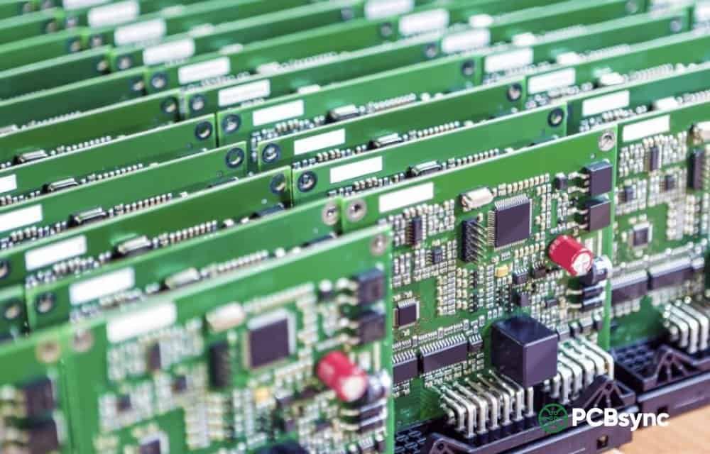
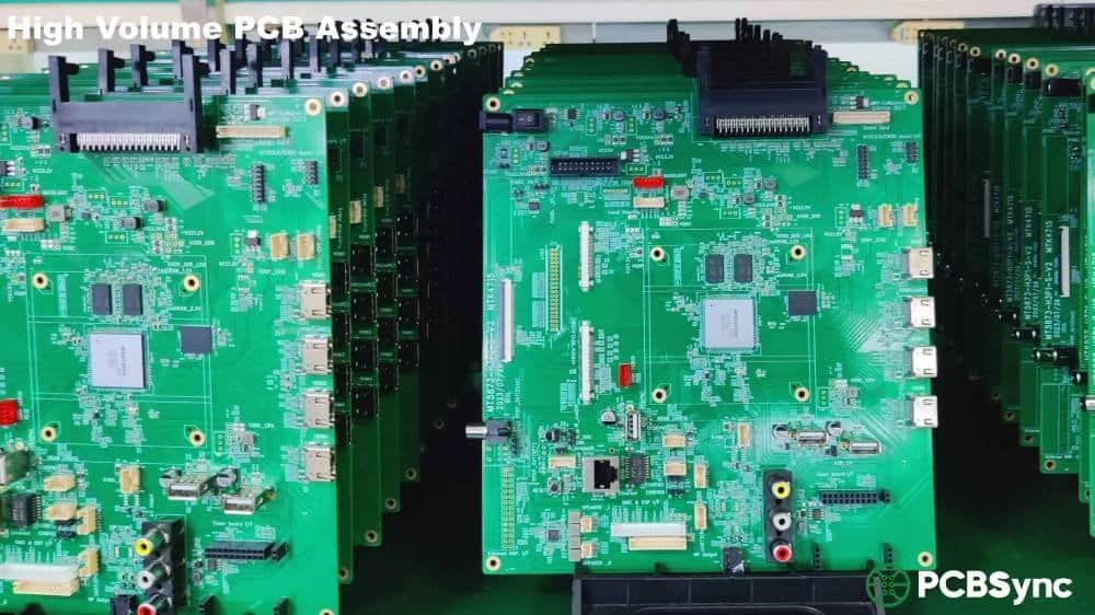
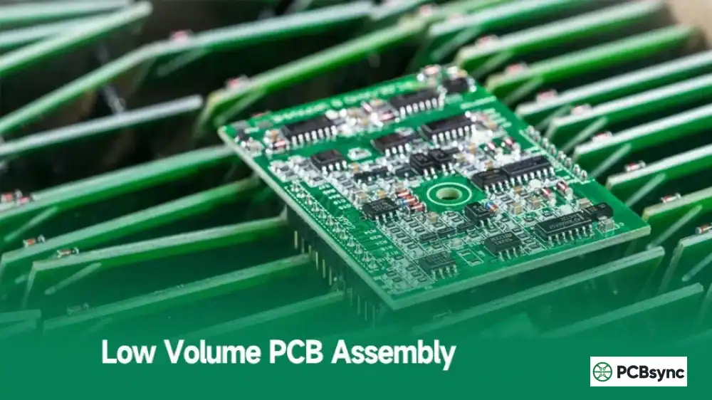
Prototype PCB assembly is the process of populating a printed circuit board with electronic components to create a functional sample for testing and validation. Unlike mass production, prototype assembly typically involves small quantities—anywhere from 1 to 50 boards—and focuses on verifying that your design works as intended before committing to large-scale manufacturing. The goal isn’t perfection on the first try; it’s learning what needs to change before you invest in production tooling and volume orders.
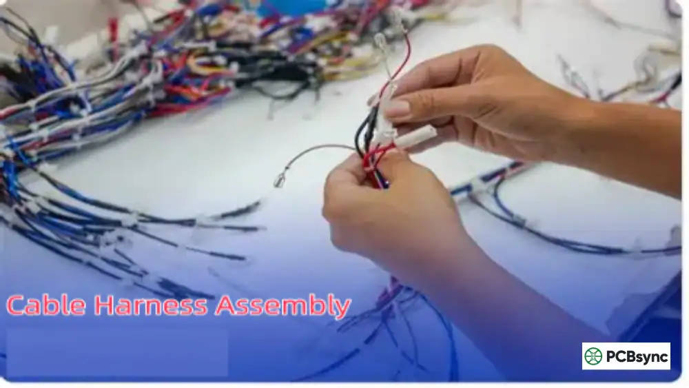
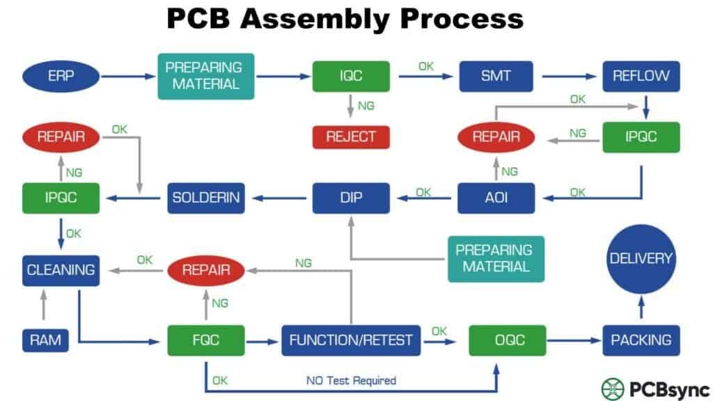
The process encompasses several stages: bare PCB fabrication, component procurement, solder paste application, component placement (either manual or automated), reflow soldering for surface-mount components, wave or hand soldering for through-hole parts, inspection, and testing. Each stage has its own potential pitfalls, which is why preparation is so critical. A problem at any stage can cascade into delays and additional costs.
It’s worth noting that the prototype phase is where you have the most flexibility. Changes that would be expensive or impossible in production are relatively easy to implement during prototyping. Take advantage of this—experiment, test edge cases, and don’t be afraid to iterate. That’s exactly what this phase is for.
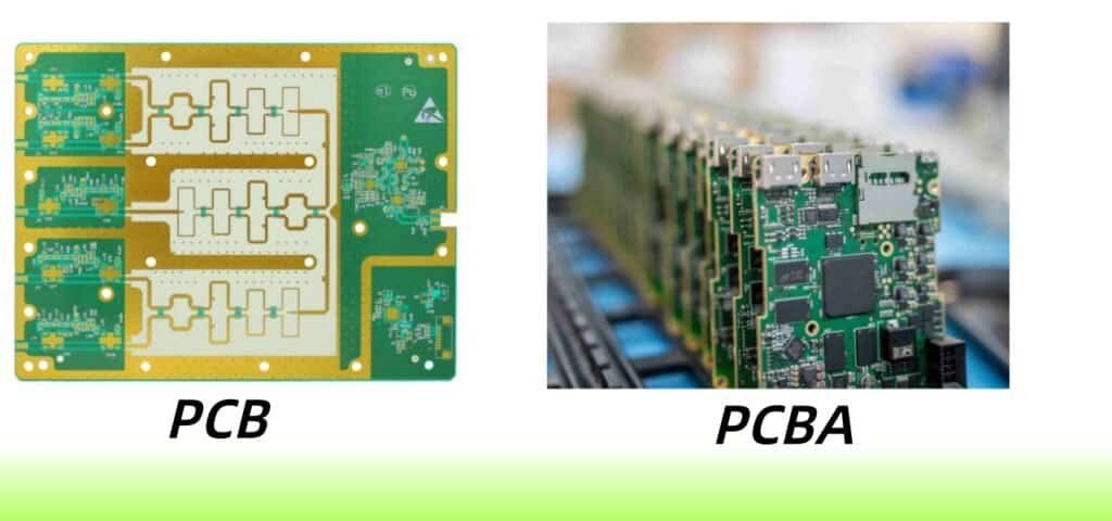
PCB Fabrication vs. PCB Assembly: Understanding the Difference
One common source of confusion is the difference between PCB fabrication and PCB assembly. Many newcomers use these terms interchangeably, but they refer to distinct processes. PCB fabrication creates the bare board with copper traces and vias, while assembly adds the components. Here’s a quick comparison:
You might be tempted to skip prototyping and go straight to production, especially if you’re confident in your design or under schedule pressure. Don’t. I’ve seen this shortcut backfire spectacularly—projects delayed by months because fundamental issues weren’t discovered until production, companies stuck with thousands of unusable boards, and budgets blown trying to fix problems that would have been cheap to address at the prototype stage.
Prototype assembly serves several critical functions that directly impact your project’s success:
Design Validation: You can simulate all day, but nothing beats powering up a real board. Prototype PCB assembly reveals issues that simulations miss—thermal problems that only appear under actual load, EMI issues from real-world trace impedances, and mechanical interferences that CAD tools don’t catch.
Component Verification: Does that footprint actually match the part? Is the thermal pad sized correctly? Does the component orientation match your silkscreen? You’ll find out during assembly. I once had a QFN package with a different pin 1 location than expected—a problem that would have been catastrophic in production.
Manufacturing Feedback: A good assembly house will catch design-for-manufacturability (DFM) issues before they become production problems. Maybe your component spacing is too tight for reliable pick-and-place, or your via-in-pad design needs adjustment. Better to find out now than during a 10,000-unit production run.
Cost Avoidance: Finding and fixing errors at the prototype stage costs a fraction of what it costs during mass production. We’re talking orders of magnitude difference. A $500 fix during prototyping becomes a $50,000 recall in production.
Tip 1: Get Your Design Files Right Before Submission
This sounds obvious, but it’s where most projects stumble. I’ve reviewed hundreds of design packages over my career, and file errors are the number one cause of delays and assembly failures. The difference between a smooth project and a frustrating one often comes down to file preparation.
Essential Files for Prototype PCB Assembly
Every assembly project requires a complete set of files that work together. Missing or mismatched files are the most common cause of delays. Here’s what you need:
File Type
Purpose
Common Mistakes
Gerber Files
Define all PCB layers including copper, mask, silk, and paste
Hole locations and sizes for vias and through-hole components
Missing plated vs non-plated distinction, wrong units
Pro tip: Run your EDA tool’s Design Rule Check (DRC) before exporting any files. Then visually inspect your Gerbers using a viewer like Gerbv or your CAD tool’s built-in viewer. I can’t count how many times I’ve caught issues just by looking at the rendered output—missing layers, incorrect apertures, or traces that didn’t connect as expected.
Bundle all files into a single ZIP archive with a clear naming convention. Sending files as separate attachments across multiple emails is a recipe for confusion and lost files. Include a readme file that lists all included files and any special instructions. Your manufacturer will thank you.
Tip 2: Follow Design for Manufacturability (DFM) Guidelines
DFM isn’t just a buzzword—it’s the difference between a board that assembles smoothly and one that causes headaches for everyone involved. Most assembly problems I’ve encountered trace back to DFM violations that could have been avoided with a bit more attention during the design phase.
Critical DFM Considerations for Prototype PCB Assembly
Component Spacing: Leave adequate clearance between components. For SMT parts, I recommend at least 0.5mm between component bodies—more if you’re using hand assembly or expect rework. This gives the pick-and-place machine room to work and makes rework possible if needed. Components packed too tightly are difficult to inspect and nearly impossible to rework without damaging adjacent parts.
Pad Design: Your pad sizes should match the component leads precisely. Too small, and you won’t get a reliable solder joint. Too large, and you risk bridging between adjacent pins. Most component manufacturers provide recommended land patterns in their datasheets—use them. When in doubt, the IPC-7351 standard provides comprehensive guidelines for pad design.
Solder Mask Clearance: Maintain at least 0.05mm (2 mil) clearance between pads. This creates a solder mask dam that prevents solder from bridging between pads during reflow. For fine-pitch components (0.5mm pitch or less), this becomes even more critical. I’ve seen entire QFP packages fail due to bridging that could have been prevented with proper solder mask design.
Fiducial Marks: Include at least three global fiducials for machine vision alignment. Place them asymmetrically so the machine can determine board orientation unambiguously. For fine-pitch components (0.5mm pitch or less), add local fiducials near those parts—the machine will use these for higher-precision placement. Fiducials should be 1mm to 3mm diameter with 3mm clearance from the board edge.
Thermal Relief: For through-hole components connected to large copper pours (like ground planes), use thermal relief connections. Without them, the thermal mass of the copper plane makes hand soldering extremely difficult—the solder won’t flow properly because the heat dissipates too quickly.
Many assembly houses offer free DFM review as part of their service. Take advantage of it. They’ll catch issues you might miss, and it’s much cheaper to fix them before fabrication than after. Some manufacturers even provide automated DFM checking tools that you can run before submitting your order.
Tip 3: Choose Components Wisely and Verify Availability
Component selection can make or break your prototype timeline. I’ve seen projects delayed by weeks because a single component was on 16-week lead time. The global chip shortage of 2020-2022 made this painfully clear to many engineers, but supply chain awareness should always be part of your design process.
Component Selection Best Practices
Check Availability First: Before finalizing your schematic, verify that key components are in stock at major distributors like Digi-Key, Mouser, Arrow, or Newark. A great design with unobtainable parts is useless. Use tools like Octopart or FindChips to compare availability across multiple distributors simultaneously.
Consider Lead Times: Semiconductors especially can have extended lead times, sometimes stretching to 52 weeks or more. If a part shows 12-week lead time, either find an alternative or factor that into your schedule. Don’t assume availability will improve—it often doesn’t.
Specify Alternatives: For passive components and common ICs, include approved alternatives in your BOM. This gives your assembler flexibility to source from available stock. Be specific about what substitutions are acceptable—a different manufacturer is usually fine for passives, but may not be for precision components.
Avoid Obsolete Parts: Check the component lifecycle status before committing. Parts marked as “Not Recommended for New Designs” or “End of Life” might work for your prototype but will cause problems when you scale to production. Some distributors have lifecycle indicators right on the product page.
Match Footprints Carefully: This is critical. A 0603 resistor won’t fit a 0402 footprint. Sounds obvious, but footprint mismatches are incredibly common, especially with IC packages that have multiple variants (QFN-32 4x4mm vs QFN-32 5x5mm, for example). Always verify the package dimensions in the datasheet against your footprint.
For turnkey prototype PCB assembly, your manufacturer will handle procurement, but you should still verify availability beforehand. You don’t want surprises after you’ve placed your order and are waiting for boards. Ask your assembler about their component sourcing—do they use only authorized distributors, or might they source from the grey market?
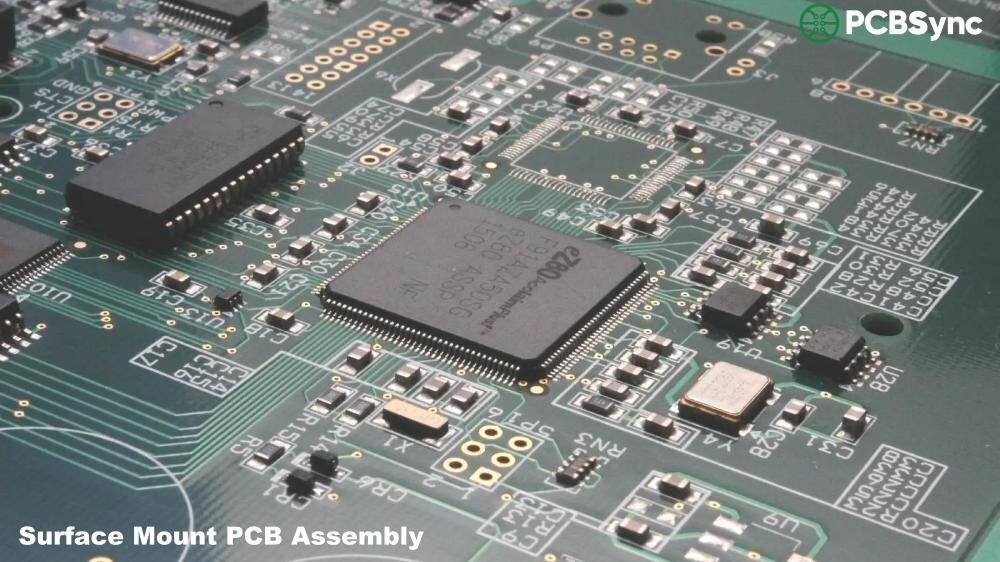
Tip 4: Select the Right Assembly Technology
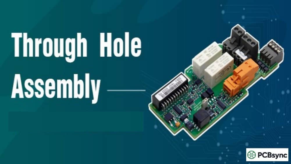
The choice between Surface Mount Technology (SMT), Through-Hole Technology (THT), and mixed assembly affects everything from cost to turnaround time to reliability. Making the right choice early in your design process can save significant time and money later.
Assembly Technology Comparison
Technology
Best For
Considerations
SMT (Surface Mount)
High-density designs, smaller form factors, automated assembly at scale
Requires reflow oven, harder to hand rework fine-pitch parts
Larger footprints, requires wave or selective soldering
Mixed Technology
Most real-world designs that combine SMT ICs with THT connectors
Requires multiple process steps, slightly higher cost and time
For prototypes, I generally recommend keeping through-hole parts to a minimum unless they’re necessary for your application—connectors that will see repeated mating cycles, high-current paths that need the additional copper area, or mechanically stressed components that benefit from the stronger joint. SMT assembly is faster, cheaper, and allows for denser layouts. Most modern components are available primarily or exclusively in SMT packages.
Tip 5: Create a Bulletproof Bill of Materials
The BOM is the Rosetta Stone of your design. It tells the assembler exactly what components go where, and any ambiguity or error will cause problems. A sloppy BOM leads to delays, wrong parts, and frustrated engineers on both ends of the relationship.
Essential BOM Elements
Every BOM should include these columns as a minimum:
Reference Designator: The unique identifier for each component placement (R1, C15, U3, etc.). Group identical parts together and list all reference designators that use that part.
Quantity: How many of this exact part are used per board. Double-check this against your schematic—it’s easy to miss a component when counting manually.
Manufacturer Part Number (MPN): The exact part number from the manufacturer, not a distributor SKU. Distributor part numbers can change; MPNs are stable identifiers.
Manufacturer Name: Especially important for parts with similar MPNs from different manufacturers. “C1206C104K5RAC” from Kemet is not the same as a similarly-numbered part from another company.
Description: A clear description including value, package, and key specifications (e.g., “10kΩ ±1% 0603 Resistor 1/10W”). This helps catch errors when the MPN doesn’t match the description.
Package/Footprint: The physical package type (0603, SOIC-8, QFN-32, etc.). This must match your PCB footprint exactly.
DNP Flag: Mark any “Do Not Populate” positions clearly with a dedicated column, not just notes in the description field.
Format your BOM as an Excel file (.xlsx) with clear column headers in the first row. Avoid merged cells—they cause import errors in procurement systems. And please, no PDFs for the primary BOM. PDF versions are fine for reference, but the working BOM should be in a format that can be imported directly into purchasing and assembly systems.
Tip 6: Partner with the Right Prototype PCB Assembly Manufacturer
Not all assembly houses are created equal. The right partner can make your project smooth and even enjoyable; the wrong one can turn it into a nightmare of delays, miscommunication, and quality issues. Choosing your manufacturing partner deserves as much thought as choosing your components.
What to Look for in an Assembly Partner
Turnaround Time: Quick-turn services range from 24 hours to 7 days. Faster isn’t always better—rushed jobs have higher error rates, and you’ll pay a premium for expedited service. Match the timeline to your actual needs. If you can afford a few extra days, the quality and cost benefits are usually worth it.
Quality Certifications: Look for ISO 9001 and IPC-A-610 compliance at minimum. These standards ensure consistent quality processes and workmanship standards. For medical or aerospace applications, you’ll need additional certifications like ISO 13485 or AS9100. Ask about their inspection processes—what percentage of boards get AOI? Do they X-ray BGA assemblies?
DFM Review Capability: A good assembler will review your design before manufacturing and flag potential issues proactively. This collaborative approach saves everyone time and money. Some even provide free automated DFM checking tools you can use before submitting.
Testing Capabilities: What testing do they offer? At minimum, you want visual inspection and continuity testing. For complex boards, look for AOI (Automated Optical Inspection), X-ray capability (essential for BGAs and hidden joints), and functional testing options. Ask whether testing is included in the base price or an additional charge.
Communication: This is often overlooked but critically important. When questions come up—and they will—you need an assembler who responds quickly and clearly. A company that takes days to answer emails will delay your project. Look for companies that assign dedicated project managers and provide direct communication channels.
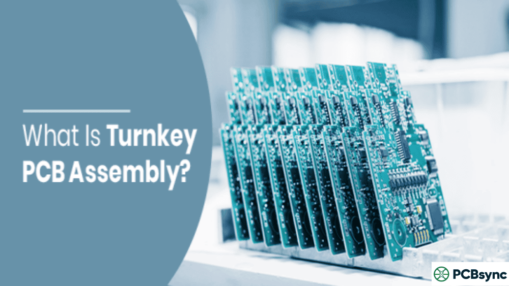
Turnkey vs. Consignment Assembly
Turnkey: The assembly house handles everything—PCB fabrication, component procurement, and assembly. This is usually the best choice for prototypes because it simplifies logistics and reduces your coordination burden. You submit files and receive finished boards. The assembler takes responsibility for the entire process.
Consignment: You provide the components (and sometimes the bare boards), and they just do the assembly. This gives you more control over component sourcing but requires more work on your end—you’re responsible for procuring everything, counting quantities, and ensuring compatibility. Only choose consignment if you have special sourcing requirements, already have parts in inventory, or need to use specific component lots for traceability.
Tip 7: Implement Thorough Testing and Plan for Iteration
Getting boards back from assembly is exciting, but the work isn’t done. Proper testing and a mindset of iteration are what separate successful projects from frustrating ones. Every prototype teaches you something—your job is to learn those lessons systematically.
Testing Hierarchy for Prototype Boards
Visual Inspection: Before powering anything, inspect every board with a magnifying glass or microscope. Look for solder bridges, cold joints (dull and grainy appearance), missing components, and wrong orientations. This five-minute check catches obvious problems before they damage anything or waste your debugging time.
Continuity and Short Tests: Use a multimeter to check critical nets for continuity and verify there are no shorts between power and ground. This takes five minutes and can save your components from going up in smoke. I once caught a manufacturing defect—a tiny copper sliver bridging power to ground—that would have destroyed every component on the board.
Power-On Sequence: Apply power gradually using a current-limited supply. Watch for excessive current draw, which indicates a short or component failure. Check that voltage rails come up correctly and in the right sequence if your design requires it. Monitor temperatures with your hand or a thermal camera—nothing should get hot immediately.
Functional Testing: Once basic power checks pass, move to functional testing. Does the microcontroller boot? Do interfaces communicate correctly? Does the analog section perform as expected? Work through your design systematically, testing each subsystem before integrating them.
Stress Testing: Subject the board to the conditions it will face in actual use—temperature extremes, voltage variations, extended operation, and mechanical stress if applicable. This reveals marginal designs that work in the lab but fail in the field. Don’t skip this step even for prototypes; it’s better to find weaknesses now.
The Iteration Mindset
Your first prototype probably won’t be perfect. That’s okay—that’s exactly why it’s a prototype and not a production unit. Document every issue you find, categorize them by severity, and prioritize fixes for the next revision. Keep a running list throughout testing, not just at the end.
Most successful products go through two to three prototype iterations before reaching production-ready status. Budget for this in your timeline and costs. Trying to get everything perfect on the first try usually takes longer than accepting iteration as part of the process. Each spin teaches you something new about your design and moves you closer to a robust final product.
Common Mistakes to Avoid in Prototype PCB Assembly
After reviewing countless prototype projects over my career, these are the mistakes I see most often. Learning from others’ errors is far cheaper than making them yourself:
Skipping Design Review: Many engineers are so eager to get boards made that they skip internal review. A second pair of eyes catches errors you’ve become blind to after staring at the same schematic for weeks.
Wrong Footprints: Especially common with package variants. That MSOP-8 isn’t the same as a SOIC-8, and QFN packages come in many different sizes with the same pin count. Double-check every footprint against the actual component datasheet.
Ignoring Thermal Requirements: Components generate heat, and that heat needs somewhere to go. If you haven’t considered thermal relief, thermal vias under hot components, or heat sinking for power devices, you’ll find out about it when the board fails or behaves erratically.
Poor Communication: Assuming the manufacturer will figure things out leads to problems. Be explicit about your requirements, especially for anything non-standard. If something matters to you, say so clearly in writing.
No Test Points: If you can’t probe it, you can’t debug it. Include test points for critical signals, power rails, and communication buses, even if space is tight. The time saved during debugging far outweighs the board area consumed.
Useful Resources for Prototype PCB Assembly
Here are tools and resources that will help you with your prototype PCB assembly projects. I use many of these regularly in my own work:
Design and Verification Tools
Gerber Viewer (Gerbv): Free, open-source Gerber viewer for verifying your design files – gerbv.github.io
Altium 365 Viewer: Free online PCB viewer for sharing and reviewing designs – altium.com/viewer
Component Sourcing and Availability
Octopart: Component search engine comparing prices and availability across distributors – octopart.com
FindChips: Real-time inventory search across global distributors – findchips.com
Digi-Key: Major distributor with extensive technical resources and datasheets – digikey.com
Mouser Electronics: Wide component selection with detailed technical information – mouser.com
Standards and Reference Materials
IPC Standards: Industry standards for PCB design, fabrication, and assembly – ipc.org
PCB Libraries: IPC-compliant footprint libraries for major EDA tools – pcblibraries.com
Saturn PCB Design Toolkit: Free calculator for trace widths, via currents, and other design parameters – saturnpcb.com/pcb_toolkit
Frequently Asked Questions About Prototype PCB Assembly
How long does prototype PCB assembly typically take?
Standard prototype PCB assembly takes 5 to 10 business days, including both fabrication and assembly. Quick-turn services can complete simple boards in 24 to 72 hours, but expect to pay a significant premium—often 2x to 3x the standard price. The actual timeline depends on board complexity (layer count, component density), component availability (parts on extended lead time can add weeks), and whether you choose turnkey or consignment assembly. Always add buffer time for shipping and potential rework. In my experience, promising stakeholders the fastest possible timeline usually backfires.
How much does prototype PCB assembly cost?
Costs vary widely based on board complexity, quantity, component count, and your choice of manufacturer. For a simple two-layer board with 50 components, expect to pay $150 to $300 for 5 assembled boards using a budget overseas manufacturer, or $400 to $800 for domestic quick-turn assembly. The total cost includes bare PCB fabrication ($5 to $50), component procurement (varies enormously), assembly labor ($50 to $200+ per board type), stencil fabrication ($20 to $100), and testing. Get quotes from multiple suppliers to compare—prices can vary by 50% or more for identical specifications.
What is the difference between SMT and through-hole assembly?
Surface Mount Technology (SMT) involves mounting components directly onto the PCB surface and using reflow soldering in an oven. It allows for smaller components, higher density designs, and efficient automated assembly. Through-Hole Technology (THT) involves inserting component leads through drilled holes and soldering on the opposite side—either by wave soldering or by hand. THT provides stronger mechanical connections and is preferred for connectors that will see repeated mating cycles, high-power components that need the additional copper area of a plated hole, and parts subject to mechanical stress. Most modern boards use a combination of both technologies.
What files do I need for prototype PCB assembly?
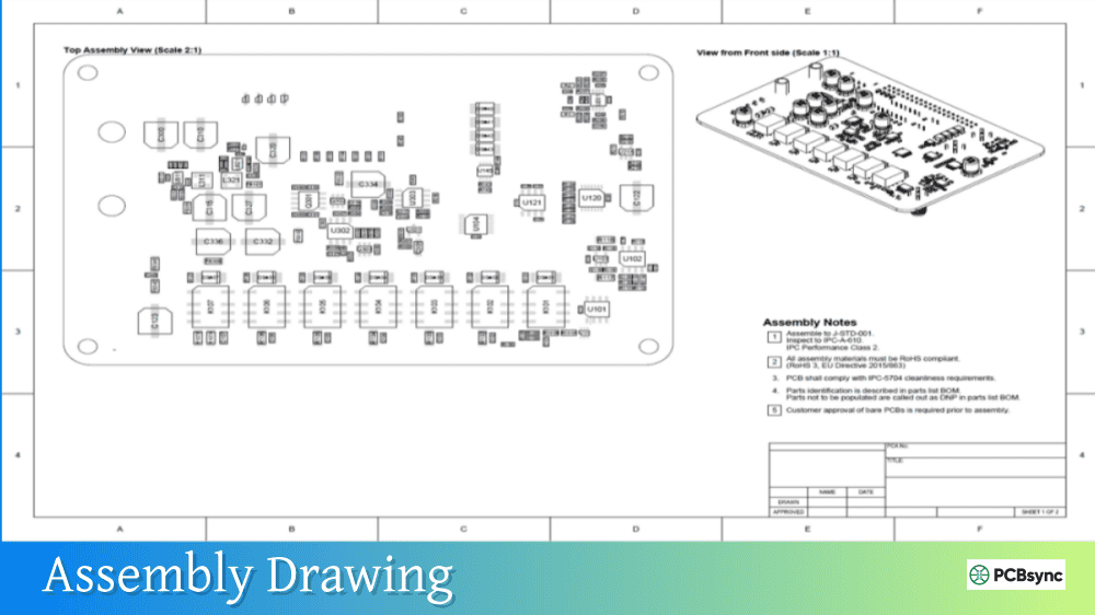
At minimum, you need Gerber files (all layers including the solder paste/stencil layer), drill files (Excellon format), a Bill of Materials in Excel format with manufacturer part numbers, and a centroid/pick-and-place file with component positions and rotations. An assembly drawing showing component placement and polarity is also helpful. Some manufacturers request the original CAD files (KiCad, Altium, Eagle) for reference. Bundle everything in a single ZIP archive and include a readme file explaining any special requirements or notes about your design.
How many prototype boards should I order?
For most projects, order 5 to 10 prototype boards. This gives you enough units for initial testing and debugging, one or two for destructive analysis or environmental testing if needed, spares in case of assembly issues or testing accidents, and samples for stakeholders, certifications, or demonstrations. The marginal cost of additional boards is usually low compared to setup costs (stencil fabrication, programming, etc.), so ordering too few can be a false economy. If your design is very stable and you’re confident in it, 3 boards might suffice. If you’re doing significant experimentation or expect multiple people to need boards simultaneously, consider 15 to 20.
Final Thoughts: Getting Your First Board Right
Prototype PCB assembly doesn’t have to be intimidating. With proper preparation, clear documentation, and the right manufacturing partner, you can get functional boards back quickly and move your project forward with confidence.
Let’s recap the seven key tips: First, prepare your design files meticulously—this prevents most common problems. Second, follow DFM guidelines to ensure your design can actually be manufactured reliably. Third, verify component availability before you finalize your design. Fourth, choose the right assembly technology for your application. Fifth, create a comprehensive and accurate BOM. Sixth, select a capable assembly partner who communicates well. And seventh, plan for systematic testing and embrace iteration as part of the development process.
Your first prototype will teach you things that no amount of simulation or planning can. Embrace that learning process, document what you discover, and apply those lessons to make your next revision even better. The goal isn’t perfection on the first try—it’s efficient learning and continuous improvement.
The engineers who succeed in this field aren’t the ones who never make mistakes—they’re the ones who catch mistakes early, learn from them quickly, and iterate efficiently. With these seven tips, you’re well on your way to joining their ranks.
Good luck with your project. Now stop reading and go build something.
Inquire: Call 0086-755-23203480, or reach out via the form below/your sales contact to discuss our design, manufacturing, and assembly capabilities.
Quote: Email your PCB files to Sales@pcbsync.com (Preferred for large files) or submit online. We will contact you promptly. Please ensure your email is correct.
Notes: For PCB fabrication, we require PCB design file in Gerber RS-274X format (most preferred), *.PCB/DDB (Protel, inform your program version) format or *.BRD (Eagle) format. For PCB assembly, we require PCB design file in above mentioned format, drilling file and BOM. Click to download BOM template To avoid file missing, please include all files into one folder and compress it into .zip or .rar format.


