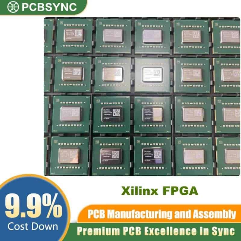
The Xilinx XC7VH580T-G2FLG1155E is a high-performance Field Programmable Gate Array (FPGA) from the Virtex-7 HT family, engineered for demanding high-bandwidth applications. Whether you are designing advanced networking systems, high-speed data acquisition platforms, or cutting-edge signal processing solutions, this device delivers exceptional logic density, ultra-fast transceivers, and robust reliability in a compact package.
What Is the Xilinx XC7VH580T-G2FLG1155E?
The XC7VH580T-G2FLG1155E belongs to Xilinx’s Virtex-7 HT (High Throughput) series — a product line specifically designed to meet the most demanding throughput requirements in modern electronics. The “HT” designation highlights its focus on high-speed serial connectivity, making it a top choice for telecommunications, data centers, and aerospace industries.
This device is manufactured on 28nm High-Performance Low-Power (HPL) technology, ensuring an excellent balance between performance and power efficiency. It is trusted by engineers worldwide seeking a Xilinx FPGA solution that scales with next-generation demands.
Technical Specifications
Core Logic & Memory
| Parameter |
Specification |
| FPGA Family |
Virtex-7 HT |
| Part Number |
XC7VH580T-G2FLG1155E |
| Logic Cells |
580,480 |
| CLB Flip-Flops |
832,000 |
| Block RAM |
1,880 × 18Kb (33.84 Mb Total) |
| DSP Slices |
1,680 |
| Process Node |
28nm HPL |
I/O & Connectivity
| Parameter |
Specification |
| Package Type |
FLG1155 (Flip-Chip BGA) |
| Total Package Pins |
1,155 |
| Max User I/O |
400 |
| GTH Transceivers |
48 (Up to 13.1 Gbps) |
| GTZ Transceivers |
8 (Up to 28.05 Gbps) |
| PCIE Interface |
Gen3 × 8 |
Power & Performance
| Parameter |
Specification |
| Speed Grade |
-2G (Extended) |
| Core Voltage (VCCINT) |
1.0V |
| Configuration Voltage |
1.8V / 3.3V |
| Operating Temperature |
0°C to +85°C (Commercial) |
| RoHS Compliance |
Yes |
Key Features & Benefits
Ultra-High-Speed Serial Transceivers
The XC7VH580T-G2FLG1155E features GTZ transceivers running at up to 28.05 Gbps, enabling 100G Ethernet and OTN (Optical Transport Network) designs without external serializer/deserializer chips.
Massive Logic Capacity
With over 580,000 logic cells and 1,680 DSP slices, this FPGA handles complex parallel processing tasks with ease, making it ideal for real-time signal processing, radar systems, and financial computing.
Advanced Memory Architecture
The on-chip Block RAM provides 33.84 Mb of fast, distributed memory, reducing latency and eliminating the need for external memory in many embedded designs.
Common Applications
-
100G/400G Ethernet Line Cards
-
Optical Transport Networking (OTN)
-
High-Performance Computing (HPC)
-
Defense & Aerospace Signal Processing
-
Test & Measurement Equipment
-
Data Center Acceleration
Why Choose the XC7VH580T-G2FLG1155E?
Engineers choose the Xilinx XC7VH580T-G2FLG1155E because it combines massive logic resources, world-class high-speed transceivers, and a proven 28nm fabrication process. Its -2G speed grade ensures reliable timing closure even in the most demanding designs. Backed by Xilinx’s comprehensive Vivado Design Suite support, development cycles are fast and efficient.