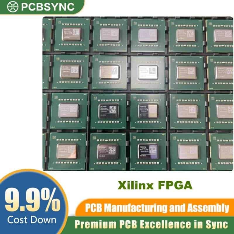
The XC7A100T-L1CSG324I is a high-performance, low-power integrated circuit from the acclaimed Artix-7 series. Designed to handle demanding embedded applications, this device provides engineers with the perfect balance of logic capacity, power efficiency, and substantial connectivity. If you are designing next-generation digital systems—ranging from industrial automation to advanced medical diagnostics—this component offers exceptional scalability and value.
What is the Xilinx XC7A100T-L1CSG324I?
At its core, the XC7A100T-L1CSG324I is an advanced Field Programmable Gate Array built on a 28nm high-k metal gate (HKMG) process. The part number reveals critical information about its specialized capabilities. The “L1” designation indicates that this is a low-power variant, operating smoothly at a reduced core voltage of 0.95V to save energy. Furthermore, the “I” suffix denotes its industrial-grade temperature rating, meaning it functions flawlessly in harsh environments ranging from -40°C to 100°C.
Housed in a compact 324-pin CSBGA package measuring just 15×15 mm, this chip allows for highly dense printed circuit board layouts without sacrificing thermal management. For developers relying on a versatile Xilinx FPGA, this particular model is highly sought after for its robust architecture and long-term reliability.
Key Technical Specifications
To make component selection easier and ensure compatibility with your system requirements, here is a breakdown of the primary technical specifications for the XC7A100T-L1CSG324I.
| Feature |
Specification |
| Manufacturer |
AMD / Xilinx |
| Device Series |
Artix-7 |
| Logic Cells |
101,440 |
| Total RAM Bits |
4,976,640 (4.86 Mb) |
| Number of I/Os |
210 |
| Operating Voltage |
0.95V – 1.05V |
| Package / Case |
324-CSBGA (15×15 mm) |
| Operating Temperature |
-40°C to 100°C (Industrial) |
Core Features and Benefits
The XC7A100T-L1CSG324I stands out in the programmable logic market due to its rich and adaptable feature set. With over 100,000 logic elements, it provides ample computational resources for complex algorithms, machine learning edge inference, and high-speed data processing. The integration of nearly 5 Mb of block RAM ensures efficient on-chip data buffering, which is an absolute necessity for digital signal processing (DSP) and intensive video routing tasks.
Additionally, the chip features powerful clock management tiles, including phase-locked loops (PLLs) and mixed-mode clock managers (MMCMs). This guarantees precise, low-jitter clocking across the entire system footprint. Its robust 210 I/O pins also support a wide voltage range (1.2V to 3.3V), making interfacing with both legacy systems and modern high-speed peripherals seamless.
Ideal Applications
Due to its optimal mix of high logic density and low power footprint, the XC7A100T-L1CSG324I is successfully deployed across multiple demanding industries. Common applications include:
-
Industrial Automation: Motor control algorithms and precise industrial protocol converters.
-
Communications: Software-defined radios (SDR) and secure, high-bandwidth data encryption modules.
-
Medical Equipment: High-resolution medical imaging and portable diagnostic devices.
-
Consumer Electronics: Advanced video processing and high-speed data acquisition systems.
Conclusion
When building cost-sensitive yet computationally demanding applications, selecting the right programmable logic is critical to your project’s overall success. The XC7A100T-L1CSG324I delivers industrial-grade reliability, impressive power efficiency, and massive logic capacity all packed into a space-saving footprint. By leveraging this versatile architecture, engineering teams can significantly accelerate their time-to-market while ensuring long-term product durability and uncompromised field performance.