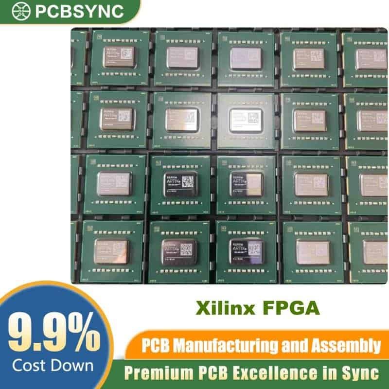
The XCV1600E-6BG560C is a high-capacity, high-performance Field Programmable Gate Array (FPGA) from Xilinx’s Virtex-E family. Manufactured on an advanced 0.18 µm, 6-layer metal CMOS process, this device delivers exceptional logic density and speed grade performance for demanding embedded design applications. Whether you are working in telecommunications, industrial automation, or high-speed signal processing, the XCV1600E-6BG560C offers the programmable logic resources to meet your design requirements.
For engineers and procurement professionals sourcing programmable logic devices, this device belongs to the broader Xilinx FPGA product ecosystem — one of the most widely deployed families in the industry.
XCV1600E-6BG560C Overview and Key Features
The XCV1600E-6BG560C is part of the Virtex-E product line, which was designed as an evolutionary advancement over the original Virtex FPGA family. The “-6” speed grade designation indicates a mid-range performance tier within the Virtex-E lineup, while the “BG560” suffix specifies the 560-pin Metal Ball Grid Array (BGA) package. The trailing “C” identifies this as the commercial temperature grade variant (0°C to 85°C junction temperature).
Why the XCV1600E-6BG560C Stands Out
The Virtex-E architecture combines a rich hierarchy of fast, flexible interconnect resources with advanced process technology to reduce time-to-market. Key differentiators include:
- High logic capacity with 34,992 logic elements and 7,776 Configurable Logic Blocks (CLBs)
- On-chip block RAM totaling 589,824 bits for data buffering and storage
- 404 user I/O pins for broad connectivity in complex system designs
- 1.8V core supply voltage for reduced power consumption
- 0.18 µm process technology delivering superior performance-to-power ratios
- Commercial temperature range (0°C – 85°C TJ) for standard industrial and consumer applications
XCV1600E-6BG560C Full Technical Specifications
The table below summarizes all critical electrical, physical, and functional parameters for the XCV1600E-6BG560C.
General Specifications Table
| Parameter |
Value |
| Manufacturer |
AMD Xilinx |
| Part Number |
XCV1600E-6BG560C |
| Series |
Virtex®-E |
| Product Category |
Embedded – FPGAs (Field Programmable Gate Array) |
| Part Status |
Obsolete |
| Speed Grade |
-6 |
Logic Resources Table
| Resource |
Quantity |
| Number of Gates |
2,188,742 |
| Number of CLBs (LABs) |
7,776 |
| Number of Logic Elements / Cells |
34,992 |
| Total RAM Bits (Block SelectRAM) |
589,824 bits |
| Number of User I/O Pins |
404 |
Electrical Characteristics Table
| Parameter |
Value |
| Supply Voltage (VCCINT) |
1.71V – 1.89V (nominal 1.8V) |
| Operating Temperature (TJ) |
0°C – 85°C |
| Process Technology |
0.18 µm CMOS |
| Metal Layers |
6-layer metal |
Package and Mechanical Specifications Table
| Parameter |
Value |
| Package Type |
560-LBGA (Exposed Pad, Metal BGA) |
| Pin Count |
560 |
| Mounting Type |
Surface Mount Technology (SMT) |
| Packaging |
Tray |
XCV1600E-6BG560C Part Number Decoder
Understanding the Xilinx part numbering convention helps engineers quickly identify the correct variant for their designs. The table below decodes each segment of the XCV1600E-6BG560C part number.
| Segment |
Meaning |
| XCV |
Xilinx Virtex FPGA family |
| 1600 |
Device size (approximately 1,600K system gates) |
| E |
Enhanced (Virtex-E generation) |
| -6 |
Speed grade (-6 = mid-range; higher number = faster) |
| BG |
Ball Grid Array package (Metal BGA) |
| 560 |
Total pin count (560 pins) |
| C |
Commercial temperature grade (0°C to 85°C) |
Virtex-E Family Architecture: What Powers the XCV1600E-6BG560C
Configurable Logic Blocks (CLBs)
Each CLB in the Virtex-E architecture consists of two slices, and each slice contains two 4-input Look-Up Tables (LUTs), flip-flops, and carry logic. This structure enables efficient implementation of arithmetic functions, state machines, and custom logic. With 7,776 CLBs, the XCV1600E-6BG560C can accommodate large and complex design hierarchies.
Block SelectRAM
The integrated block SelectRAM provides 589,824 bits of on-chip memory distributed throughout the device. Each SelectRAM block can be independently configured as a simple dual-port or single-port RAM. This eliminates the need for external memory in many buffering and FIFO applications, improving system integration and reducing PCB complexity.
SelectI/O Technology
The 404 user I/O pins of the XCV1600E-6BG560C support multiple I/O standards through Xilinx’s SelectI/O technology. This flexible I/O infrastructure allows the device to interface with a wide range of external components and bus standards without requiring external level shifters in many designs.
Dedicated DLL Circuits
The Virtex-E family includes dedicated Delay-Locked Loop (DLL) circuits to eliminate clock distribution delays. These DLLs enable zero-delay clock distribution, frequency synthesis, and phase shifting — critical capabilities in high-speed synchronous designs.


