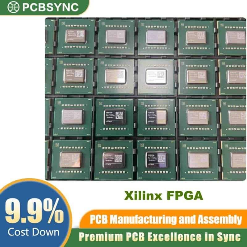
The XC7VX1140T-L2FLG1930E is a high-end Virtex-7 XT family FPGA manufactured by Xilinx (now AMD) on a 28 nm high-performance low-power (HPL), high-k metal gate (HKMG) process. Designed for applications that demand the highest logic density and serial bandwidth, this device delivers 1,139,200 logic cells, 96 GTH transceivers, and up to 1.4 Tb/s of total I/O bandwidth. Because it uses Xilinx Stacked Silicon Interconnect (SSI) technology, the XC7VX1140T-L2FLG1930E integrates multiple Super Logic Regions (SLRs) into a single package, giving engineers ASIC-class capacity in a fully programmable fabric.
Overview of the XC7VX1140T-L2FLG1930E
This part is the low-voltage (0.9 V), speed-grade -2 variant in the extended temperature range, supplied in the 1,930-ball flip-chip BGA (FLG1930) package. The “L2” designation means it operates at a reduced core voltage to cut static power by roughly 50% compared with previous-generation Virtex-6 devices, while still hitting a -2 speed grade. As a result, the XC7VX1140T-L2FLG1930E suits power-sensitive wireline, test and measurement, ASIC prototyping, and high-performance computing designs.
Key Features and Benefits
Moreover, the device combines dense programmable logic with a rich mix of hardened IP. Engineers get 3,360 DSP48E1 slices for signal processing, 67,680 Kb of block RAM for on-chip buffering, and four integrated PCI Express Gen3 x8 blocks for host connectivity. Additionally, dual 12-bit XADC analog inputs enable on-chip monitoring without external ADCs.
Technical Specifications
Core Logic Resources
| Parameter |
Value |
| Logic cells |
1,139,200 |
| CLB slices |
178,000 |
| CLB flip-flops |
1,424,000 |
| Max distributed RAM |
17,700 Kb |
| DSP48E1 slices |
3,360 |
Memory, Clocking & Hard IP
| Parameter |
Value |
| Block RAM (36 Kb blocks) |
1,880 |
| Total block RAM |
67,680 Kb (≈67.7 Mb) |
| CMTs (MMCM + PLL) |
24 |
| PCIe Gen3 hard blocks |
4 |
| XADC (12-bit, 1 MSPS) |
2 channels |
I/O and Serial Transceivers
| Parameter |
Value |
| Max user I/O |
1,100 |
| GTH transceivers |
96 |
| GTH line rate |
600 Mb/s – 13.1 Gb/s |
| Total I/O bandwidth |
1.4 Tb/s |
| Peak DSP performance |
4.7 TMAC/s |
Package & Electrical
| Parameter |
Value |
| Package |
FLG1930 (Pb-free FCBGA, 1,930 balls) |
| Process technology |
28 nm HKMG HPL |
| Speed grade |
-2L (low voltage) |
| Core voltage (VCCINT) |
0.9 V |
| Temperature range |
Extended (E) |
Typical Applications
Consequently, the XC7VX1140T-L2FLG1930E is widely deployed in 100G/400G networking line cards, wireless backhaul and baseband units, radar and electronic warfare systems, medical imaging front ends, broadcast video processing, and ASIC/SoC emulation platforms where massive gate counts and serial connectivity are essential.
Where to Source the XC7VX1140T-L2FLG1930E
For authentic stock, full traceability, and competitive pricing on this device and related parts, visit the Xilinx FPGA catalog for current availability and datasheet support.