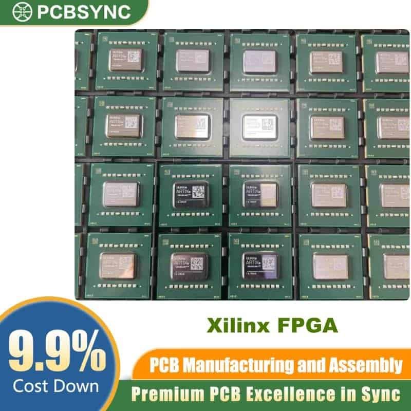
The XC7VX1140T-1FLG1930C is the flagship device of the Xilinx Virtex-7 XT family, delivering the highest logic density, signal-processing throughput, and serial-bandwidth per watt available on the 28 nm 7-Series platform. Built on TSMC’s 28 nm HKMG HPL process and assembled with Stacked Silicon Interconnect (SSI) technology across four Super Logic Regions (SLRs), the XC7VX1140T-1FLG1930C packs 1,139,200 logic cells into a single 1930-ball FCBGA package — making it the go-to choice for ASIC prototyping, wireless test equipment, defense radar, high-frequency trading, broadcast video, and 100G/400G line-card designs.
Why Designers Choose the XC7VX1140T-1FLG1930C
This commercial-grade (0 °C to 85 °C), -1 speed-grade device combines 67,680 Kb of block RAM, 3,360 DSP48E1 slices (4.7 TMAC/s peak), and 96 GTH transceivers running up to 13.1 Gb/s — enough aggregate bandwidth to drive multiple 100GbE ports, CPRI fronthaul, or JESD204B converter farms from a single chip. Four integrated PCIe Gen3 x8 hard blocks, 24 clock management tiles, and 1,100 SelectIO pins (DDR3 up to 1,866 Mb/s) round out a feature set that fully programmable alternatives to ASSPs and ASICs rarely match. Compared to the previous Virtex-6 generation, the XC7VX1140T-1FLG1930C cuts static power roughly in half while doubling system performance.
Key Applications
- 100G/400G Ethernet bridging, OTN switching, and packet processing
- 4G/5G wireless baseband and Massive-MIMO remote radio heads
- High-end test & measurement (oscilloscopes, logic analyzers, BERTs)
- Software-defined radio (SDR) and electronic warfare platforms
- Medical imaging back-ends and ASIC emulation systems
For broader family information and additional package/speed-grade options, see our complete Xilinx FPGA inventory.
XC7VX1140T-1FLG1930C Technical Specifications
Logic & Memory Resources
| Parameter |
Value |
| Manufacturer |
Xilinx (AMD) |
| Family / Series |
Virtex-7 XT |
| Process Technology |
28 nm HKMG HPL |
| Logic Cells |
1,139,200 |
| CLB Slices |
178,000 |
| CLB Flip-Flops |
1,424,000 |
| Max Distributed RAM |
17,700 Kb |
| Block RAM Blocks (36 Kb) |
1,880 |
| Total Block RAM |
67,680 Kb (67.68 Mb) |
| DSP48E1 Slices |
3,360 |
I/O, Transceivers & Clocking
| Parameter |
Value |
| GTH Transceivers (max 13.1 Gb/s) |
96 |
| PCIe Hard Blocks (Gen3 x8) |
4 |
| Clock Management Tiles (CMTs) |
24 |
| User I/O Pins |
1,100 |
| I/O Banks |
22 |
| XADC (12-bit, 1 MSPS, dual ADC) |
1 |
Package & Ordering Information
| Parameter |
Value |
| Package |
1930-ball FCBGA (FLG1930) |
| Body Size |
45 mm × 45 mm |
| Ball Pitch |
1.0 mm |
| Speed Grade |
-1 |
| Temperature Grade |
C (Commercial, 0 °C to +85 °C) |
| RoHS / Lead-Free |
Yes (Pb-free, exemption 15) |
| Configuration |
JTAG, SPI, BPI, SelectMAP, Serial |
| Security |
256-bit AES + HMAC/SHA-256, SEU detection |