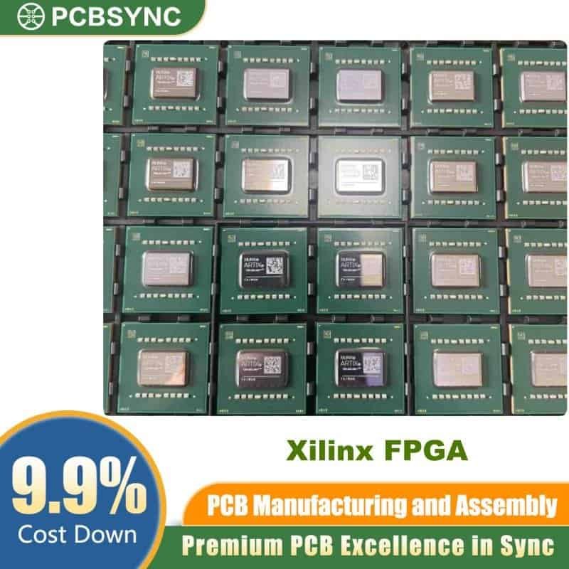
Overview of XC2S200-6FGG987C FPGA Technology
The XC2S200-6FGG987C is a powerful field-programmable gate array (FPGA) from AMD Xilinx’s proven Spartan-II family, delivering exceptional performance for embedded systems, telecommunications, and industrial automation applications. This commercial-grade FPGA combines 200,000 system gates with advanced programmable logic capabilities, making it an ideal choice for engineers seeking cost-effective, high-density solutions.
As part of the renowned Xilinx FPGA portfolio, the XC2S200-6FGG987C represents a superior alternative to traditional mask-programmed ASICs, offering field-upgradeable functionality without hardware replacement requirements.
Key Specifications and Technical Features
Core Architecture Specifications
| Specification |
Value |
| System Gates |
200,000 gates |
| Logic Cells |
5,292 cells |
| CLB Array Configuration |
28 x 42 (1,176 total CLBs) |
| Maximum User I/O |
284 pins |
| Distributed RAM |
75,264 bits |
| Block RAM |
56 Kbits |
| Operating Voltage |
2.5V |
| Speed Grade |
-6 (highest performance) |
| Process Technology |
0.18μm CMOS |
| Operating Frequency |
Up to 263 MHz |
Package and Environmental Details
| Parameter |
Specification |
| Package Type |
Fine-pitch Ball Grid Array (FBGA) |
| Total Pins |
987 balls |
| Temperature Range |
Commercial (0°C to +85°C) |
| RoHS Compliance |
Lead-free available (G suffix) |
| Pb-free Option |
Yes |
Advanced FPGA Capabilities
Programmable Logic Resources
The XC2S200-6FGG987C delivers remarkable flexibility through its comprehensive logic resources:
- 5,292 logic cells enable complex digital circuit implementation
- 1,176 Configurable Logic Blocks (CLBs) arranged in optimized 28×42 array
- Four Delay-Locked Loops (DLLs) for precise clock management
- 284 user I/O pins supporting multiple interface standards
- Dual-column Block RAM architecture for high-speed data buffering
Memory Architecture
| Memory Type |
Capacity |
Application |
| Distributed RAM |
75,264 bits |
Fast look-up tables, small buffers |
| Block RAM |
56 Kbits |
Data buffering, FIFO, packet processing |
| Total On-Chip Memory |
131,264 bits |
Combined storage resources |
Applications and Use Cases
Telecommunications Equipment
The XC2S200 FPGA excels in communication systems requiring high-speed data processing, protocol implementation, and signal manipulation capabilities for network routers and transmission devices.
Industrial Automation and Control
Ideal for motor control systems, process automation, and machinery control applications where precise digital logic and real-time processing are critical requirements.
Digital Signal Processing
With 200,000 system gates and dedicated block RAM, this FPGA handles complex DSP algorithms for audio processing, image processing, and data acquisition systems.
Embedded Vision Systems
The combination of high logic density and embedded memory enables efficient image processing algorithms for robotics, surveillance, and medical imaging applications.
Design and Development Tools
Software Support
- Vivado Design Suite – Modern development environment
- ISE Design Tools – Legacy support for Spartan-II devices
- IP Core Integration – Pre-verified intellectual property blocks
- Simulation Tools – ModelSim, ISIM compatibility
Development Resources
Engineers working with the XC2S200-6FGG987C benefit from comprehensive development board options including ZedBoard, Basys 3, Nexys4-DDR, and Digilent Arty S7 platforms for rapid prototyping and validation.
Advantages Over Traditional ASICs
Cost-Effective Development
The XC2S200-6FGG987C eliminates expensive NRE (non-recurring engineering) costs associated with ASIC development, while avoiding lengthy fabrication cycles and inherent manufacturing risks.
Field Programmability
Unlike fixed ASICs, this FPGA supports in-field design upgrades and modifications without physical hardware replacement, reducing lifecycle costs and extending product longevity.
Rapid Time-to-Market
Programmable logic enables iterative design refinement and faster product deployment compared to traditional ASIC workflows.
Performance and Reliability Features
High-Speed Operation
The -6 speed grade designation ensures optimal performance under demanding operational conditions, supporting applications requiring maximum clock frequencies up to 263 MHz.
Robust I/O Capabilities
With 284 maximum user I/O pins, the XC2S200 provides extensive interfacing options for sensors, actuators, communication protocols, and peripheral devices.
Power Efficiency
The 2.5V core voltage and 0.18μm process technology deliver balanced performance-per-watt characteristics suitable for power-conscious embedded applications.
Ordering and Availability Information
Part Number Breakdown
XC2S200-6FGG987C decoding:
- XC2S200 – Spartan-II family, 200K gates
- 6 – Speed grade (highest performance)
- FGG – Fine-pitch BGA, lead-free packaging
- 987 – Pin count
- C – Commercial temperature range
Package Options Comparison
| Package |
Pin Count |
Dimensions |
I/O Available |
| FGG987 |
987 balls |
TBD |
284 maximum |
| FGG456 |
456 balls |
27x27mm |
284 maximum |
| FG256 |
256 balls |
17x17mm |
176 maximum |
| PQG208 |
208 pins |
QFP |
140 maximum |
Technical Support and Documentation
Available Resources
Engineers can access comprehensive technical documentation including:
- Complete datasheet specifications (DS001)
- Application notes and design guides
- Reference designs and IP cores
- Pinout diagrams and PCB layout guidelines
- Timing analysis and constraint files
Community and Support
The Spartan-II XC2S200 benefits from extensive community support through FPGA forums, developer networks, and official AMD Xilinx technical support channels.
Competitive Alternatives and Cross-References
Family Comparisons
| Device |
System Gates |
Logic Cells |
Block RAM |
Max I/O |
| XC2S150 |
150,000 |
3,888 |
48K |
260 |
| XC2S200 |
200,000 |
5,292 |
56K |
284 |
| XC2S300E |
300,000 |
6,912 |
72K |
329 |
Upgrade Path
For designs requiring additional resources, consider the Spartan-IIE (XC2S300E) or Spartan-3 families offering enhanced capabilities while maintaining development tool compatibility.
Conclusion
The XC2S200-6FGG987C Spartan-II FPGA delivers an exceptional balance of logic density, I/O capability, and cost-effectiveness for modern digital design challenges. With 200,000 system gates, 5,292 logic cells, and comprehensive development tool support, this FPGA enables engineers to create sophisticated embedded systems, communication platforms, and industrial control solutions.
Whether developing high-speed data acquisition systems, wireless baseband processors, or automated control equipment, the XC2S200 provides the programmable logic resources and performance characteristics required for success in demanding applications.


