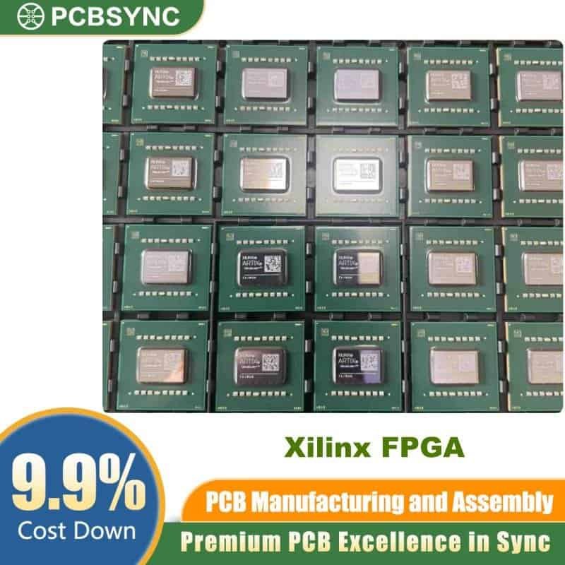
The XC2S200-6FGG977C represents a powerful solution in the Xilinx Spartan-II FPGA family, delivering exceptional programmable logic performance for demanding applications. This field-programmable gate array combines 200,000 system gates with advanced features, making it an ideal choice for engineers seeking a cost-effective alternative to traditional ASICs.
Overview of XC2S200-6FGG977C FPGA
The XC2S200-6FGG977C is a member of Xilinx’s proven Spartan-II family, featuring premium speed grade -6 performance in a fine-pitch BGA package. This programmable logic device eliminates the substantial upfront costs and lengthy development cycles associated with mask-programmed ASICs while offering field-upgradeable capabilities that traditional solutions cannot match.
Key Specifications at a Glance
| Specification |
Value |
| Part Number |
XC2S200-6FGG977C |
| Family |
Spartan-II FPGA |
| System Gates |
200,000 |
| Logic Cells |
5,292 |
| Speed Grade |
-6 (Fastest Commercial) |
| Package Type |
FGG456 (456-Ball Fine-Pitch BGA) |
| Operating Voltage |
2.5V |
| Technology Node |
0.18μm |
| Temperature Range |
Commercial (0°C to 85°C) |
Technical Architecture and Performance
Configurable Logic Block (CLB) Array
The XC2S200-6FGG977C features a robust 28 x 42 CLB matrix, providing 1,176 total configurable logic blocks. This architecture enables complex digital designs with:
- High logic density for sophisticated algorithms
- Flexible routing resources for optimized signal paths
- Distributed RAM capabilities totaling 75,264 bits
- Dedicated block RAM of 56K bits for efficient data storage
Input/Output Capabilities
| I/O Feature |
Specification |
| Maximum User I/O |
284 pins |
| I/O Standards Support |
Multiple LVTTL, LVCMOS, and other standards |
| Voltage Compatibility |
Flexible I/O banking |
| Global Clock Inputs |
4 dedicated clock pins |
Advanced Features of the Spartan-II XC2S200
Delay-Locked Loop (DLL) Technology
The XC2S200-6FGG977C incorporates four Delay-Locked Loops positioned strategically at each corner of the die. These DLLs provide:
- Precise clock distribution and deskewing
- Reduced clock-to-output delays
- Enhanced timing performance across the device
Memory Architecture
Distributed RAM
With 75,264 bits of distributed RAM, designers can implement:
- Small, fast lookup tables
- FIFO buffers
- Shift registers
- Custom memory configurations
Block RAM
The 56K bits of dedicated block RAM enable:
- Efficient data buffering
- Packet storage for communication protocols
- Coefficient storage for DSP applications
Applications and Use Cases
The XC2S200-6FGG977C excels in various demanding applications:
Digital Signal Processing
- Audio processing and filtering
- Image processing pipelines
- Real-time video processing
- Custom DSP algorithm implementation
Communication Systems
- Protocol implementation and conversion
- Data encoding/decoding engines
- Channel coding and error correction
- Network packet processing
Control and Automation
- Industrial control systems
- Motor control applications
- Sensor interface and data acquisition
- Programmable logic controllers (PLCs)
Consumer Electronics
- Set-top boxes
- Digital cameras and imaging devices
- Gaming peripherals
- Smart home devices
Package Information: FGG456 Fine-Pitch BGA
| Package Characteristic |
Details |
| Total Ball Count |
456 balls |
| Package Technology |
Fine-Pitch Ball Grid Array |
| Footprint |
Optimized for high I/O density |
| Thermal Performance |
Enhanced heat dissipation |
| Assembly |
Suitable for automated PCB assembly |
Speed Grade -6: Maximum Performance
The -6 speed grade designation indicates this is the fastest commercial temperature range option for the XC2S200 device. This premium performance tier delivers:
- Reduced propagation delays through logic elements
- Faster maximum operating frequencies up to 263 MHz
- Improved setup and hold times for critical timing paths
- Optimized for high-performance applications requiring maximum speed
Why Choose XC2S200-6FGG977C Over ASICs?
Cost Advantages
- No NRE (Non-Recurring Engineering) costs unlike ASIC development
- Lower upfront investment for product development
- Reduced financial risk for new projects
Development Benefits
- Rapid prototyping capabilities with immediate implementation
- Iterative design refinement without silicon respins
- Shorter time-to-market compared to ASIC development cycles
Flexibility Advantages
- Field upgradeable through reconfiguration
- Design modifications without hardware changes
- Product lifecycle extension through firmware updates
Design Tools and Support
Working with the XC2S200-6FGG977C is streamlined through comprehensive Xilinx development tools:
- ISE Design Suite for synthesis and implementation
- ChipScope Pro for in-system debugging
- Timing analysis tools for performance optimization
- IP core libraries for accelerated development
For comprehensive resources on Xilinx FPGA development and implementation strategies, designers can access extensive documentation and community support.
Power Consumption Characteristics
| Power Parameter |
Typical Value |
| Core Voltage (VCCINT) |
2.5V |
| I/O Voltage (VCCO) |
2.5V to 3.3V |
| Quiescent Current |
Low static power |
| Dynamic Power |
Proportional to design activity |
Reliability and Quality
The XC2S200-6FGG977C meets rigorous quality standards:
- Proven Spartan-II architecture with extensive field deployment
- Industrial-grade manufacturing processes
- Comprehensive testing and quality assurance
- Long-term availability for production planning
Comparison with Other Spartan-II Family Members
| Device |
System Gates |
Logic Cells |
Total CLBs |
Max I/O |
| XC2S50 |
50,000 |
1,728 |
384 |
176 |
| XC2S100 |
100,000 |
2,700 |
600 |
176 |
| XC2S150 |
150,000 |
3,888 |
864 |
260 |
| XC2S200 |
200,000 |
5,292 |
1,176 |
284 |
Getting Started with XC2S200-6FGG977C
Development Board Options
Engineers can leverage various evaluation platforms:
- Custom adapter PCBs for prototyping
- JTAG programming interfaces
- Development kits with peripheral support
Programming Methods
- JTAG boundary scan programming
- Master/Slave serial configuration
- SelectMAP parallel programming
- SPI-based configuration options
Conclusion
The XC2S200-6FGG977C delivers an optimal balance of performance, flexibility, and cost-effectiveness for advanced digital design projects. With 200,000 system gates, premium -6 speed grade performance, and comprehensive I/O capabilities in a fine-pitch BGA package, this Spartan-II FPGA provides engineers with a proven platform for implementing sophisticated digital systems without the constraints of traditional ASIC development.
Whether you’re developing communication systems, implementing digital signal processing algorithms, or creating custom control solutions, the XC2S200-6FGG977C offers the resources and performance needed for successful project completion.


