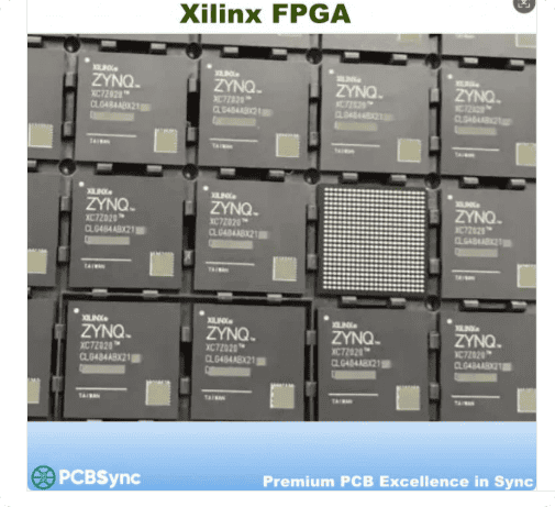
Overview of XC2S200-6FGG929C FPGA
The XC2S200-6FGG929C is a powerful field-programmable gate array (FPGA) from Xilinx’s renowned Spartan-II family. This versatile programmable logic device delivers exceptional performance for cost-sensitive applications requiring high-density logic implementation. With 200,000 system gates and advanced features, the XC2S200-6FGG929C stands as an optimal choice for telecommunications, automotive, consumer electronics, and industrial control systems.
Key Technical Specifications
| Specification |
Details |
| Product Family |
Spartan-II |
| System Gates |
200,000 |
| Logic Cells |
4,704 |
| Package Type |
FGG929 (Fine-Pitch Ball Grid Array) |
| Speed Grade |
-6 (Standard Performance) |
| I/O Pins |
624 user I/O |
| Operating Voltage |
2.5V core, 3.3V I/O |
| Configuration Memory |
SRAM-based |
Advanced Features and Capabilities
Programmable Logic Architecture
The XC2S200-6FGG929C incorporates Xilinx’s proven FPGA architecture, featuring configurable logic blocks (CLBs) that enable complex digital circuit implementation. Each logic cell contains look-up tables (LUTs), flip-flops, and dedicated routing resources, ensuring optimal performance for diverse applications.
Memory Resources
| Memory Type |
Capacity |
| Block RAM |
56 Kbits |
| Distributed RAM |
Available in CLBs |
| RAM Blocks |
14 blocks × 4K bits |
Clock Management System
The device features four delay-locked loops (DLLs) providing:
- Precise clock distribution
- Clock multiplication and division
- Phase shifting capabilities
- Reduced clock skew across the device
Performance Characteristics
Speed and Timing
| Performance Metric |
Value |
| Speed Grade |
-6 |
| Maximum Frequency |
Up to 200 MHz (design-dependent) |
| Propagation Delay |
Optimized for high-speed operation |
| I/O Standards Supported |
LVTTL, LVCMOS, PCI, GTL, SSTL, HSTL |
FGG929 Package Benefits
Physical Specifications
The Fine-Pitch Ball Grid Array (FGG929) package offers superior advantages:
- Total Pins: 929 balls
- User I/O: 624 configurable pins
- Package Size: Compact footprint for dense PCB layouts
- Thermal Performance: Enhanced heat dissipation
- Signal Integrity: Minimal parasitic effects
Pin Configuration Advantages
The FGG929 package maximizes I/O availability, making the XC2S200-6FGG929C ideal for applications requiring extensive connectivity, including multi-channel data acquisition, video processing, and complex communication protocols.
Application Areas
Telecommunications and Networking
The XC2S200-6FGG929C excels in:
- Protocol conversion and bridging
- Digital signal processing (DSP) implementations
- Network packet processing
- Data encryption and security
Industrial Control Systems
Perfect for:
- Motor control and automation
- Sensor interface and processing
- Real-time control loops
- Machine vision systems
Consumer Electronics
Optimal for:
- Video and image processing
- Audio codec implementation
- Display controllers
- Gaming peripherals
Design Tools and Software Support
| Tool Category |
Support |
| Design Entry |
ISE Design Suite, Schematic capture, VHDL/Verilog |
| Simulation |
ModelSim, ISim |
| Synthesis |
XST (Xilinx Synthesis Technology) |
| Place & Route |
ISE Implementation tools |
| Programming |
iMPACT, JTAG configuration |
Power Consumption Profile
Operating Conditions
| Power Parameter |
Typical Value |
| Core Voltage (VCCINT) |
2.5V ±5% |
| I/O Voltage (VCCO) |
1.5V to 3.3V |
| Standby Current |
Low power mode available |
| Dynamic Power |
Design-dependent |
Configuration Options
The XC2S200-6FGG929C supports multiple configuration modes:
- Master Serial Mode: Independent configuration
- Slave Serial Mode: Controlled by external processor
- JTAG Mode: Boundary-scan testing and programming
- SelectMAP Mode: Parallel configuration for faster boot times
Quality and Reliability
Environmental Specifications
| Parameter |
Range |
| Operating Temperature |
0°C to +85°C (Commercial) |
| Storage Temperature |
-65°C to +150°C |
| Humidity |
10% to 90% non-condensing |
| MTBF |
High reliability rating |
Why Choose XC2S200-6FGG929C?
Cost-Effective Performance
The Spartan-II architecture delivers exceptional value, balancing performance requirements with budget constraints. The XC2S200-6FGG929C provides enterprise-grade functionality at competitive pricing.
Extensive I/O Capability
With 624 user I/O pins in the FGG929 package, this FPGA handles complex interface requirements without external expansion, reducing overall system cost and board space.
Proven Technology
Backed by Xilinx’s industry leadership, the Spartan-II family has demonstrated reliability across millions of deployed units worldwide. The XC2S200-6FGG929C inherits this proven track record.
Integration and Development
PCB Design Considerations
- Ball Pitch: Fine-pitch requires advanced PCB fabrication
- Layer Count: Typically 6-10 layers recommended
- Decoupling: Multiple capacitors near power pins
- Thermal Management: Adequate cooling solution required
Development Resources
Engineers working with the XC2S200-6FGG929C benefit from:
- Comprehensive datasheets and user guides
- Reference designs and application notes
- Active developer community
- Technical support from Xilinx and distributors
Comparison With Other Density Options
| Feature |
XC2S200 Advantage |
| Logic Density |
200K gates – ideal mid-range solution |
| I/O Count (FGG929) |
Maximum flexibility for connectivity |
| Price/Performance |
Optimized for most applications |
| Development Time |
Extensive tool support reduces time-to-market |
Getting Started with XC2S200-6FGG929C
Development Kit Options
To accelerate your design process:
- Evaluation Boards: Available from Xilinx and third-party vendors
- Programming Cables: Platform Cable USB for JTAG configuration
- Software: ISE WebPACK (free version) or ISE Foundation/Professional
Design Flow Overview
- Specification: Define functional requirements
- HDL Coding: Write VHDL or Verilog code
- Simulation: Verify logic functionality
- Synthesis: Convert HDL to netlist
- Implementation: Place and route design
- Programming: Configure the FPGA
Where to Source XC2S200-6FGG929C
For reliable procurement and technical support of Xilinx FPGA solutions, partnering with authorized distributors ensures genuine components, proper handling, and warranty coverage.
Conclusion
The XC2S200-6FGG929C represents a compelling FPGA solution for engineers seeking robust performance, extensive I/O capabilities, and cost-effective implementation. Its 200,000 system gates, combined with the 929-pin ball grid array package, provide the resources needed for demanding applications across telecommunications, industrial, and consumer markets.
Whether you’re developing next-generation communication equipment, implementing sophisticated control algorithms, or creating innovative consumer products, the XC2S200-6FGG929C delivers the programmable logic capabilities, flexibility, and reliability your project demands.


