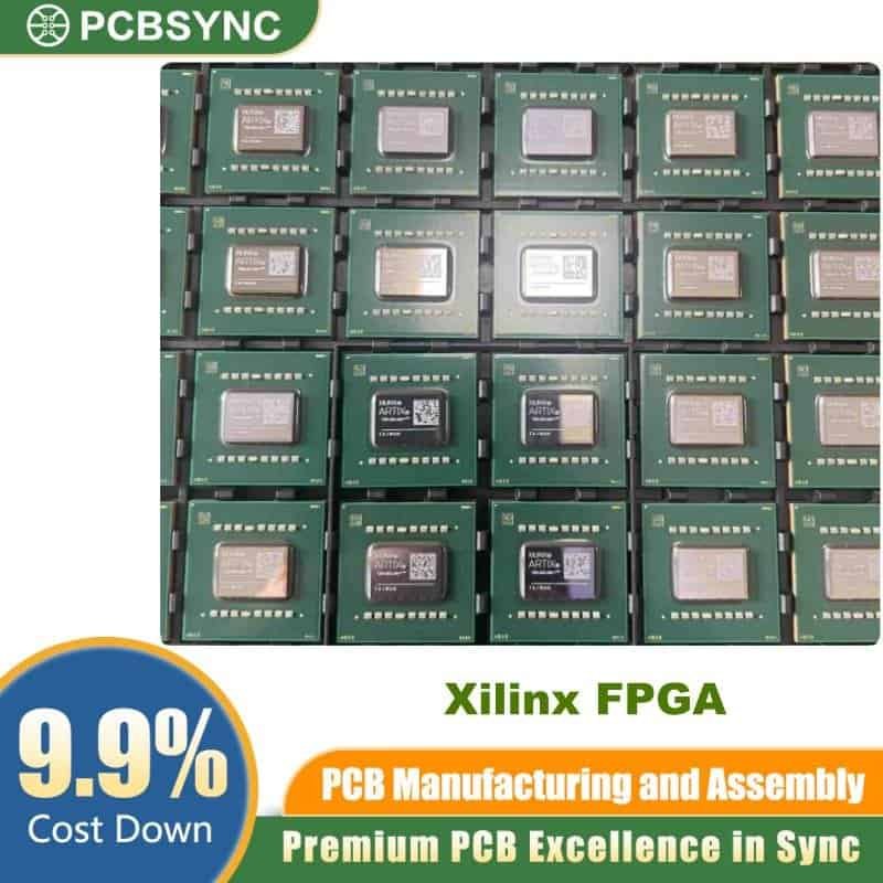
The XC2S200-6FGG1508C is a powerful member of the Spartan-II FPGA family originally developed by Xilinx (now AMD). Designed for cost-sensitive yet performance-demanding applications, this FPGA delivers flexible programmable logic, making it an excellent alternative to traditional ASIC solutions.
Built on a 0.18μm CMOS process, this device combines high logic density, efficient memory architecture, and reliable operation across industrial and commercial environments. It is widely used in embedded systems, industrial automation, telecommunications, and digital signal processing.
Key Features of XC2S200-6FGG1508C
Advanced Programmable Logic Architecture
The XC2S200 series offers robust logic resources, enabling designers to implement complex digital systems with ease.
- Up to 200,000 system gates
- 5,292 logic cells for flexible design implementation
- Fully reprogrammable architecture for iterative development
High-Speed Performance
With a -6 speed grade, this FPGA supports high-frequency applications and optimized timing performance.
- Clock performance up to ~200 MHz
- Fast interconnect architecture for predictable timing
Rich Memory Resources
The integrated memory structure supports both distributed and block RAM configurations.
- 57,344 total RAM bits
- Dual-port block RAM for efficient data handling
Flexible I/O Capabilities
The device supports a wide range of I/O standards for versatile system integration.
- Up to 284 user I/O pins
- Multiple interface standards for compatibility
XC2S200-6FGG1508C Specifications Table
| Parameter |
Specification |
| FPGA Family |
Spartan-II |
| System Gates |
200,000 |
| Logic Cells |
5,292 |
| CLBs |
1,176 |
| RAM |
57,344 bits |
| Max I/O |
284 |
| Speed Grade |
-6 |
| Core Voltage |
2.5V |
| Operating Temperature |
0°C to 85°C |
| Package Type |
FBGA (Fine-Pitch BGA) |
Specifications are based on the XC2S200 series architecture.
Architecture Overview
Configurable Logic Blocks (CLBs)
The FPGA consists of an array of CLBs, each containing logic cells capable of implementing combinational and sequential logic. This modular structure ensures scalability and design flexibility.
Clock Management with DLLs
The XC2S200 incorporates Delay-Locked Loops (DLLs) to enhance clock stability, reduce skew, and improve system synchronization.
Efficient Routing System
A segmented routing architecture ensures low power consumption and high-speed signal propagation across the device.
Electrical Characteristics
| Parameter |
Value |
| Core Voltage (VCCINT) |
2.375V – 2.625V |
| I/O Voltage (VCCO) |
1.5V – 3.3V |
| Process Technology |
0.18μm |
| Mounting Type |
Surface Mount |
Applications of XC2S200-6FGG1508C
This FPGA is ideal for a wide range of applications, including:
- Embedded control systems
- Industrial automation
- Telecommunications equipment
- Consumer electronics
- Digital signal processing (DSP)
Its reprogrammable nature allows engineers to update designs without hardware replacement, significantly reducing development risk and cost.
Advantages Over ASIC Solutions
| Feature |
FPGA (XC2S200) |
ASIC |
| Development Cost |
Low |
High |
| Time-to-Market |
Fast |
Slow |
| Flexibility |
Reprogrammable |
Fixed |
| Risk |
Low |
High |
Why Choose XC2S200-6FGG1508C?
The XC2S200-6FGG1508C stands out due to its balance of performance, flexibility, and cost-efficiency. It enables rapid prototyping and scalable production, making it a preferred choice for engineers seeking reliable FPGA solutions.
Despite being part of an older FPGA generation, it remains relevant for legacy systems, maintenance projects, and cost-sensitive designs where proven stability is essential.