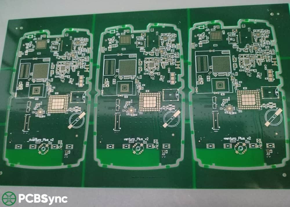
Precision Engineered for High-Performance Electronics
When your design demands reliability, signal integrity, and flawless surface finish, the PCBSync 1.6mm ENIG 8 Layer PCB stands in a class of its own. Built for engineers and product developers who refuse to compromise, this multilayer board combines advanced fabrication technology with industry-leading materials to deliver consistent, repeatable results — from prototype to full production run.
Superior Stackup Architecture
At the heart of this product is an 8-layer stackup engineered to maximize signal routing density while minimizing electromagnetic interference. The standard 1.6mm total board thickness provides the structural rigidity required for demanding mechanical environments, making it ideal for industrial control systems, telecommunications hardware, medical instrumentation, and high-speed computing applications. Each layer is precision-laminated under controlled temperature and pressure conditions, ensuring uniform dielectric spacing and exceptional bond strength throughout the entire board structure.
ENIG Surface Finish — The Gold Standard
PCBSync utilizes Electroless Nickel Immersion Gold (ENIG) as the surface finish, and for good reason. ENIG delivers a flat, solderable surface that is perfectly suited for fine-pitch components, Ball Grid Arrays (BGAs), and surface-mount technology (SMT) pads. The nickel barrier layer — typically 3–6 µm thick — prevents copper diffusion, while the immersion gold layer — ranging from 0.05 to 0.1 µm — protects against oxidation and ensures outstanding solderability over an extended shelf life. The result is a board that performs impeccably through reflow soldering, wave soldering, and hand-soldering processes alike.
Built to Rigorous Specifications
Every PCBSync 8 Layer PCB is manufactured in compliance with IPC Class 2 and Class 3 standards, with full traceability across the production process. Key manufacturing parameters include a minimum trace width and spacing of 3/3 mil, controlled impedance tolerance within ±10%, and a via aspect ratio optimized for reliable plating. Copper weight options range from 1 oz to 2 oz per layer, giving designers the flexibility to handle both signal-level and power-distribution requirements within a single board.
The FR-4 dielectric material offers a glass transition temperature (Tg) of 150°C or higher, making the board resilient in thermally demanding environments. Boards undergo 100% electrical testing, automated optical inspection (AOI), and X-ray verification for buried and blind via integrity before shipment.
Fast Turnaround, Scalable Volume
PCBSync understands that speed matters. Standard lead times start from 5 business days, with express options available for time-critical projects. Whether you need a handful of engineering samples or tens of thousands of production units, PCBSync scales seamlessly without sacrificing quality.
The Right Choice for Complex Designs
From RF shielding layers and dedicated power planes to high-speed differential pairs and dense BGA fanouts, the PCBSync 1.6mm ENIG 8 Layer PCB gives you every tool you need to bring sophisticated electronics to life. Trust the board that professionals trust — precise, durable, and ready to perform.