Inquire: Call 0086-755-23203480, or reach out via the form below/your sales contact to discuss our design, manufacturing, and assembly capabilities.
Quote: Email your PCB files to Sales@pcbsync.com (Preferred for large files) or submit online. We will contact you promptly. Please ensure your email is correct.
Notes: For PCB fabrication, we require PCB design file in Gerber RS-274X format (most preferred), *.PCB/DDB (Protel, inform your program version) format or *.BRD (Eagle) format. For PCB assembly, we require PCB design file in above mentioned format, drilling file and BOM. Click to download BOM template To avoid file missing, please include all files into one folder and compress it into .zip or .rar format.
If you’ve spent any time in electronics manufacturing, you’ve probably heard terms like PCB, PWB, and PCBA thrown around interchangeably. I’ve been working with circuit boards for over a decade, and I still see confusion about these terms—even among experienced engineers. The truth is, while these acronyms sound similar and often refer to the same physical object, they represent different stages and concepts in electronics manufacturing.
Today, I want to clear up this confusion once and for all. Whether you’re sourcing components, communicating with manufacturers, or just trying to understand technical documentation, knowing the difference between these terms can save you headaches and costly mistakes.
What is a PCB (Printed Circuit Board)?
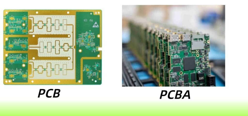
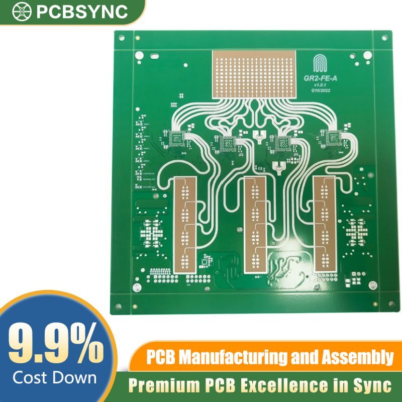
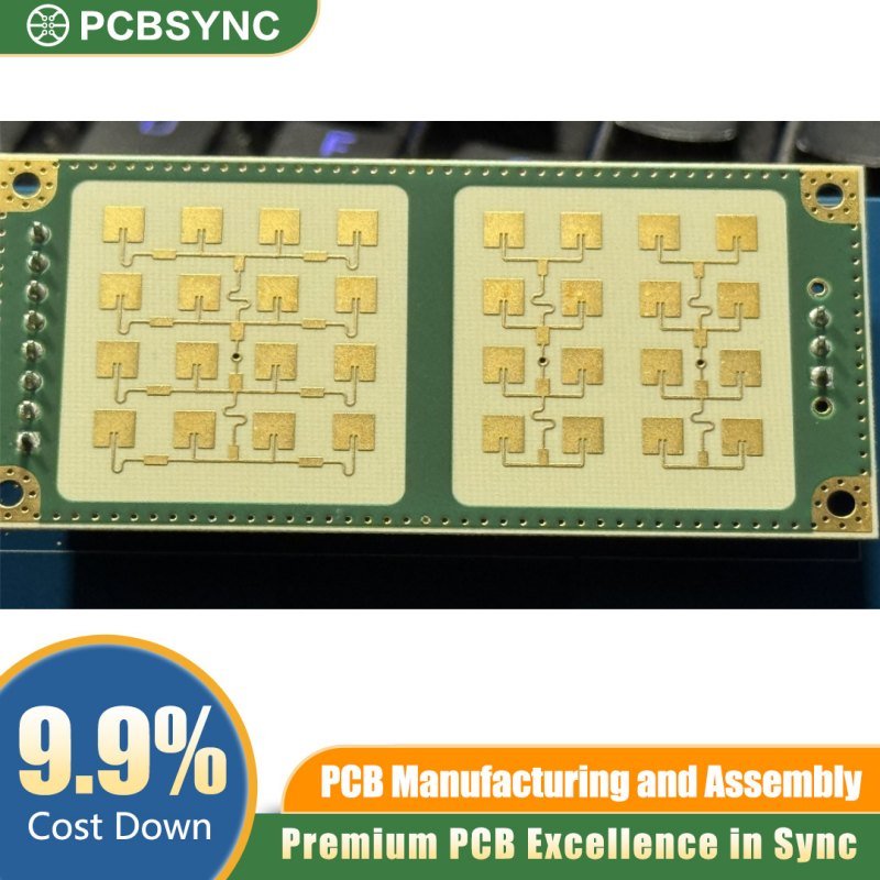
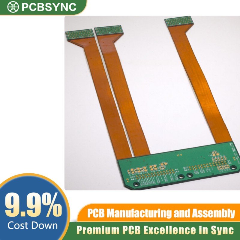
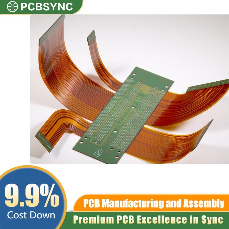
Let’s start with the most common term: PCB, or Printed Circuit Board. When I say “PCB,” I’m talking about the foundational board that mechanically supports and electrically connects electronic components. Think of it as the skeleton and nervous system of any electronic device combined into one.
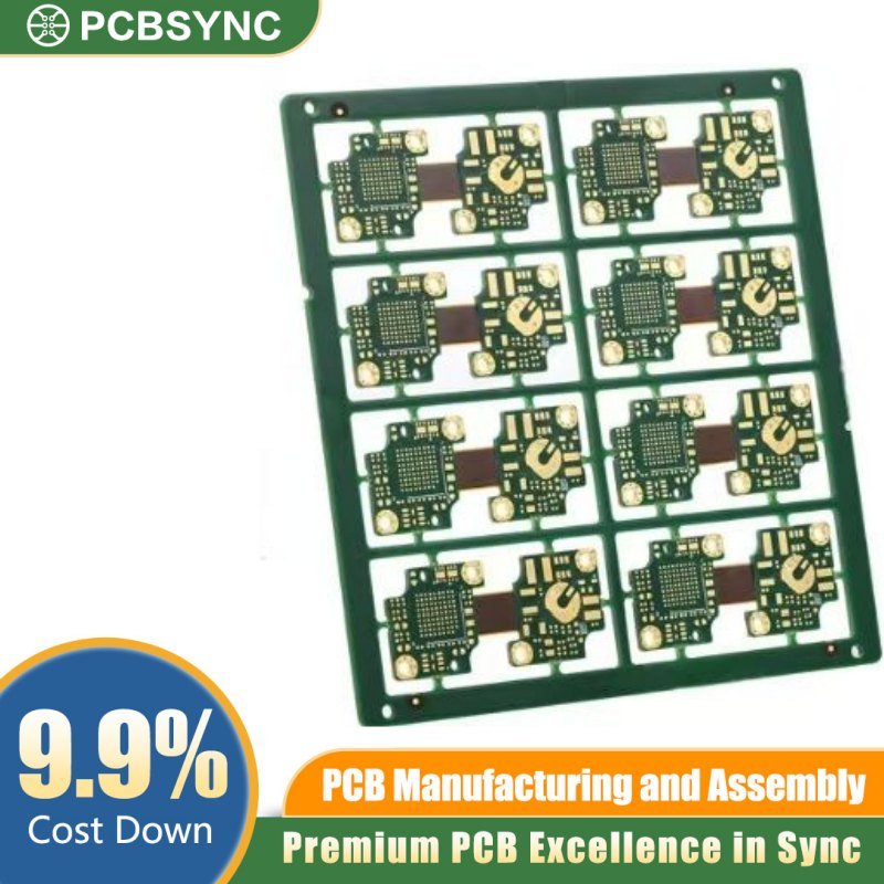
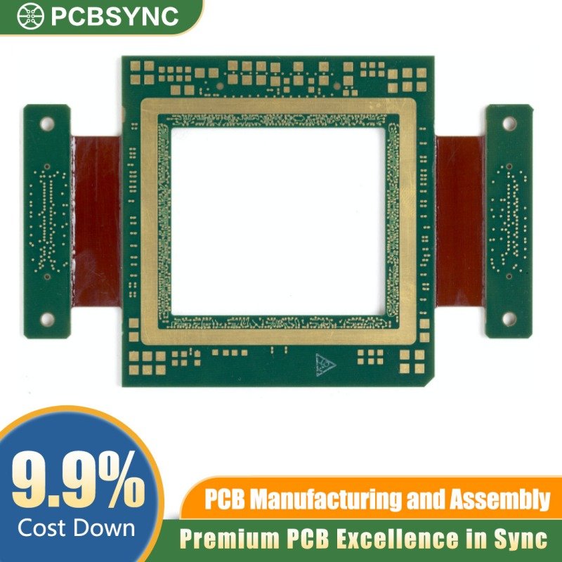
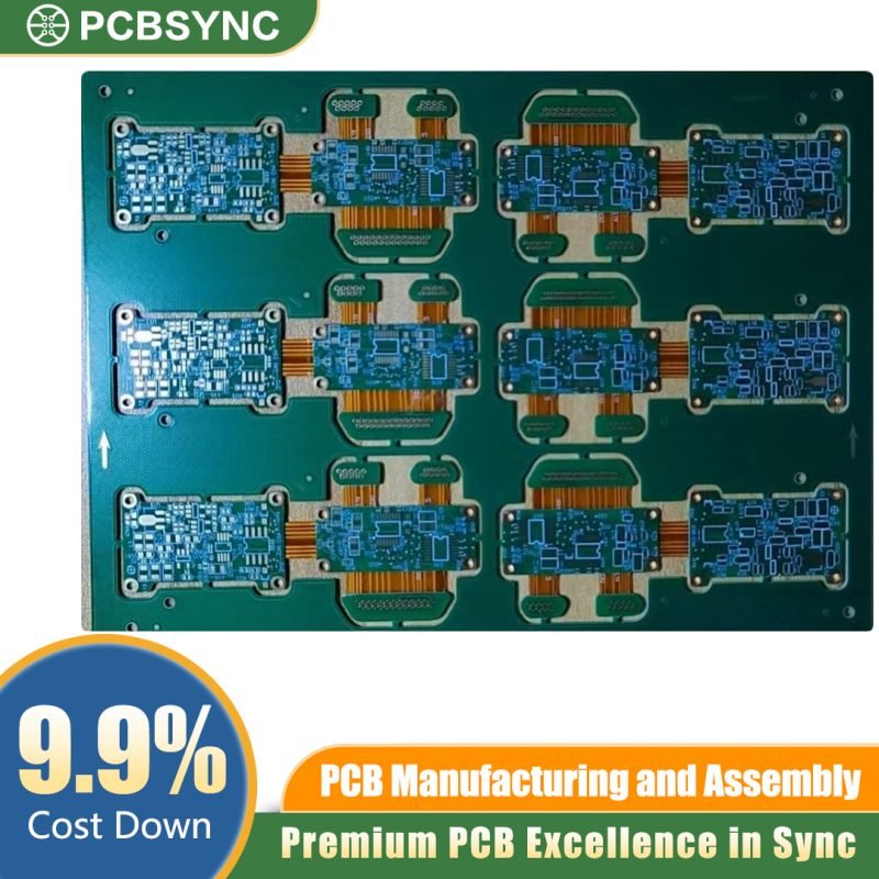
A PCB consists of copper layers laminated onto a non-conductive substrate—typically FR-4 fiberglass material. These copper layers are etched into specific patterns to create conductive pathways, called traces, that connect different points on the board. The non-conductive substrate provides mechanical strength and electrical isolation between layers.
Here’s what makes up a typical PCB:
Substrate Layer: Usually made from FR-4 (Flame Retardant 4), which is a composite material made of woven fiberglass cloth with an epoxy resin binder. This provides the rigid structure.
Copper Layers: These conductive layers carry electrical signals between components. You can have anywhere from one layer (single-sided PCB) to 30+ layers in complex applications like aerospace systems.
Solder Mask: The green (or sometimes blue, red, or black) coating you see on most circuit boards. This protects the copper traces from oxidation and prevents solder bridges during assembly.
Silkscreen: The white lettering and symbols printed on top of the solder mask. This legend identifies components, test points, and provides assembly instructions.
The term “Printed Circuit Board” has become the global standard. When you order a “PCB” from any manufacturer worldwide—whether in China, the United States, or Germany—they know exactly what you’re talking about. The IPC (Association Connecting Electronics Industries) standards, including IPC-2221 and IPC-6012, all officially use “PCB” as the standard terminology.
In my experience, about 95% of technical documentation, datasheets, and industry communications use PCB as the default term. It’s simply become the lingua franca of electronics manufacturing.
Now, here’s where things get interesting. PWB stands for Printed Wiring Board, and historically, it was actually the original term used in the electronics industry.
Back in 1903, when the patent for the early circuit board was filed, it was called “Printed Wire.” These early boards were simple—they just provided point-to-point connections without any components mounted on the surface. The term “Printed Wiring Board” or PWB was widely used when circuit boards first entered mass production.
So what’s the practical difference between PWB and PCB? Honestly, in most contexts today, there isn’t one. Both terms refer to the same thing: a bare board with conductive pathways ready for component assembly.
However, some engineers (myself included, in certain contexts) use PWB to specifically emphasize the “bare board” state—meaning the board without any components soldered onto it. Think of it as the clean canvas before the painting begins.
The term PWB is still actively used in:
Japan: This is the big one. Japanese manufacturers often prefer PWB over PCB because “PCB” is also the abbreviation for polychlorinated biphenyls, a harmful industrial chemical. To avoid confusion and potential regulatory complications, many Japanese electronics companies stick with PWB in their documentation.
Military and Aerospace: Some military specifications and aerospace documentation still use PWB, particularly in legacy systems and older technical manuals.
Academic Settings: Universities teaching circuit board fundamentals sometimes use PWB when distinguishing between the bare board substrate and the assembled product.
I’ve worked with Japanese suppliers where all the technical drawings, specifications, and communication referred to PWBs. When you understand this is just their regional preference for the same thing we call a PCB, it suddenly makes sense.
What is a PCBA (Printed Circuit Board Assembly)?
Here’s where the distinction becomes crystal clear and actually matters in practical terms. PCBA stands for Printed Circuit Board Assembly, and it refers to a PCB that has been fully populated with electronic components.
Think of the progression this way:
PCB/PWB = The bare board (just the substrate and copper traces)
PCBA = The complete assembly (board + all components soldered on)
When you crack open your smartphone, laptop, or any electronic device, you’re looking at a PCBA—not just a PCB. The board has resistors, capacitors, integrated circuits, connectors, and countless other components all soldered into place.
The assembly process typically involves two main technologies:
Surface Mount Technology (SMT): This is the modern standard where tiny components are placed directly onto pads on the board’s surface and then soldered using reflow ovens. SMT allows for much higher component density and is what enables our smartphones to pack incredible functionality into tiny spaces.
Through-Hole Technology (THT): The older method where component leads are inserted through drilled holes in the board and soldered on the opposite side. This is still used for components that need extra mechanical strength, like large connectors or high-power components.
In my purchasing experience, when you request a quote from a contract manufacturer, you need to be specific: Are you ordering bare PCBs or complete PCBAs? The price difference is massive. A bare PCB might cost $5-10, while the same board as a PCBA could cost $50-100 or more, depending on component complexity.
The industry standardized on “PCBA” as the official term for assembled boards after 1999, when various standards organizations updated their terminology. Before that, you’d see PWA (Printed Wiring Assembly), PCA (Printed Circuit Assembly), and other variants. Today, PCBA is the universally recognized term for a populated board.
Let me break this down in a way that’ll stick with you:
PCB = PWB ≠ PCBA
PCB and PWB are essentially the same thing—a bare board. PCBA is fundamentally different—it’s the completed assembly.
Here’s a practical comparison:
Aspect
PCB/PWB
PCBA
Components
None (bare board)
Fully populated with components
Manufacturing Stage
Fabrication complete
Assembly complete
Ready to Use
No
Yes (after testing)
Cost
Lower ($2-50 typical)
Higher ($20-500+ typical)
Lead Time
Shorter (3-10 days)
Longer (2-6 weeks)
Testing Required
Basic electrical test
Functional testing required
When terminology matters most:
In procurement and manufacturing, using the wrong term can cause real problems. I’ve seen purchase orders get delayed because someone ordered “PCBs” when they actually needed “PCBAs,” leading to weeks of confusion and rush assembly work.
In technical documentation, if you’re writing assembly instructions or service manuals, being precise matters. Tell a technician to “replace the PCB” when you mean “replace the PCBA,” and you might have them trying to desolder dozens of components unnecessarily.
Related Terms You Should Know
The electronics industry loves acronyms, and there are a few more related to circuit boards that you’ll encounter:
PCA (Printed Circuit Assembly): This is essentially synonymous with PCBA. You’ll see PCA used in older documentation and by some European manufacturers. It means the same thing—an assembled board.
CCA (Circuit Card Assembly): Another term for PCBA, though “CCA” is less common. It’s sometimes used in aerospace and computing contexts where the board is more “card-like” in form factor, like computer expansion cards.
PWA (Printed Wiring Assembly): This is the historical term for what we now call PCBA. It follows the same logic as PWB→PCB evolution. You’ll rarely see this in modern documentation unless you’re dealing with military or legacy systems.
Bare Board: This is simply a plain-English way of saying PCB or PWB. When someone says “bare board,” they definitely mean without components.
Populated Board: Informal term for PCBA—a board with components on it.
In my experience, sticking with PCB (for bare boards) and PCBA (for assembled boards) will serve you well 99% of the time. These are the globally recognized, IPC-standard terms that virtually everyone understands.
Regional and Industry Variations
Understanding regional preferences can make your international dealings much smoother:
United States and Europe: PCB is the standard term, used almost universally. PCBA for assembled boards.
Japan: PWB is preferred for bare boards, largely due to the PCB/polychlorinated biphenyls confusion mentioned earlier. They also use PWBA (Printed Wiring Board Assembly) more often than PCBA.
China: Interestingly, Chinese manufacturers use PCB exclusively in English communication, even when their internal documentation might use different characters. If you’re sourcing from China, always use PCB and PCBA—it’s what they expect.
Military and Defense: U.S. military specifications (MIL-SPECs) sometimes still reference PWB and PWA, particularly in older equipment documentation. However, even the military has been transitioning to PCB terminology in recent years.
How to Choose the Right Terminology
Here’s my practical advice after years of working across different companies and countries:
For everyday communication: Use PCB for bare boards and PCBA for assembled boards. This is the safest, most universally understood approach.
When working with Japanese partners: Be aware they might use PWB, and don’t be confused by it. Feel free to use their terminology in correspondence—it shows cultural awareness.
In technical documentation: Be absolutely precise. If you’re writing specifications, use:
“Bare PCB” or “unpopulated PCB” when referring to boards without components
“PCBA” or “assembled PCB” when referring to populated boards
Avoid ambiguity that could lead to manufacturing errors
In purchasing: Always clarify in your RFQ (Request for Quote) whether you need bare boards or assembled boards. I typically write something like: “Quote request for bare PCB fabrication only” or “Quote request for complete PCBA (PCB + assembly).”
Understanding the Manufacturing Flow
To really grasp these terms, it helps to understand how circuit boards are made:
Stage 1: PCB Design – Engineers create the circuit schematic and board layout using CAD software like Altium, Eagle, or KiCAD.
Stage 2: PCB Fabrication – The bare board is manufactured. This involves:
Printing the copper pattern onto the substrate
Etching away unwanted copper
Drilling holes for through-hole components and vias
Applying solder mask and silkscreen
Electrical testing
At the end of Stage 2, you have a PCB/PWB—a bare board.
Stage 3: PCBA Assembly – Components are added:
Solder paste is applied to SMT pads (usually via stencil)
Pick-and-place machines position SMT components
Reflow oven melts the solder to create connections
Through-hole components are inserted (manual or automated)
Wave soldering or hand soldering for through-hole parts
Cleaning and inspection
Functional testing
At the end of Stage 3, you have a PCBA—a complete assembly ready for integration.
Many manufacturers offer both services (fab + assembly), while others specialize in just one. Knowing the correct terminology helps you find the right partner and get accurate quotes.
Frequently Asked Questions (FAQs)
1. Is there any functional difference between a PCB and a PWB?
No, PCB and PWB refer to the exact same physical object—a bare circuit board with conductive traces but no components. The difference is purely historical and regional. PWB was the original term used in the 1940s-1950s, while PCB has become the modern global standard. Some regions, particularly Japan, still prefer PWB to avoid confusion with the toxic chemical also abbreviated as PCB (polychlorinated biphenyls). In your day-to-day work, you can treat these terms as interchangeable when referring to bare boards.
2. Can I use the term PCB to refer to an assembled board?
Technically, no—but in casual conversation, many people do. Formally, a PCB is a bare board without components, while a PCBA is the assembled version. However, in everyday speech, you’ll often hear engineers say “PCB” even when they mean the assembled board, relying on context to clarify. In documentation, purchasing, or technical communication, always use PCBA when you mean an assembled board to avoid confusion. I’ve seen costly mistakes happen when procurement teams ordered “PCBs” thinking they’d get assembled boards, only to receive bare boards instead.
3. What’s the typical cost difference between PCB and PCBA?
This varies enormously based on complexity, but as a rough guide: a simple 2-layer bare PCB might cost $2-10 per board in moderate quantities (100-1000 pieces). The same board as a PCBA with components could cost $20-100+ depending on component complexity and count. High-end PCBAs with hundreds of components, advanced ICs, and fine-pitch parts can easily run into hundreds of dollars per unit. The assembly labor, component procurement, testing, and additional quality control all add significant cost to the final PCBA price.
4. Which term should I use in my technical documentation?
Use PCB when referring to the bare board substrate and PCBA when referring to the populated assembly. Be consistent throughout your documentation. If you need to be extra clear, use qualifiers like “bare PCB,” “unpopulated PCB,” “assembled PCBA,” or “populated PCBA.” In bills of materials (BOMs), clearly distinguish between the PCB item (the board itself) and the PCBA item (the complete assembly). Most professional documentation follows IPC standards, which use PCB and PCBA as the official terms.
5. Do I need different manufacturers for PCB fabrication and assembly?
Not necessarily. Many manufacturers offer both services as “turnkey” solutions—you provide them with your design files and BOM, and they handle both PCB fabrication and assembly. However, some companies specialize in just one service. High-volume production often uses specialized fab houses for boards and separate assembly houses, while prototyping and low-volume work typically goes to companies offering both services. The advantage of using a single source is simplified communication and logistics; the advantage of separating them is potentially lower costs and access to specialists for each process.
Conclusion
After reading this guide, you should now understand that PCB and PWB are essentially synonyms for a bare circuit board, with PWB being the historical and regionally preferred term in some areas. PCBA, on the other hand, represents a fundamentally different stage—the complete assembly with all components soldered in place.
In 2026, the electronics industry continues to standardize around PCB and PCBA as the primary terms, with IPC standards, global manufacturers, and technical documentation all adopting this nomenclature. While you might encounter PWB in Japanese documentation or legacy military specs, understanding the context will help you navigate these variations without confusion.
The key takeaway? When communicating about circuit boards, be specific:
Use PCB or bare PCB for boards without components
Use PCBA or assembled PCB for populated boards
Clarify terminology in international communication
Always specify what you need in purchasing and technical documents
Master these distinctions, and you’ll communicate more effectively with manufacturers, avoid costly procurement mistakes, and demonstrate professionalism in technical documentation. After all, precision in language leads to precision in manufacturing—and that’s what we’re all aiming for.
Additional Resources
For deeper understanding of PCB design and manufacturing, I recommend these resources:
IPC Standards (www.ipc.org): IPC-2221 (Generic Standard on Printed Board Design), IPC-6012 (Qualification and Performance Specification for Rigid Printed Boards)
Industry Publications: Circuit Cellar Magazine, PCB007 Magazine
Online Communities: EEVblog Forums, Reddit r/PrintedCircuitBoard, All About Circuits forums
These resources have been invaluable in my own engineering career and continue to provide up-to-date information on PCB technologies, manufacturing techniques, and industry best practices.
Inquire: Call 0086-755-23203480, or reach out via the form below/your sales contact to discuss our design, manufacturing, and assembly capabilities.
Quote: Email your PCB files to Sales@pcbsync.com (Preferred for large files) or submit online. We will contact you promptly. Please ensure your email is correct.
Notes: For PCB fabrication, we require PCB design file in Gerber RS-274X format (most preferred), *.PCB/DDB (Protel, inform your program version) format or *.BRD (Eagle) format. For PCB assembly, we require PCB design file in above mentioned format, drilling file and BOM. Click to download BOM template To avoid file missing, please include all files into one folder and compress it into .zip or .rar format.


