Inquire: Call 0086-755-23203480, or reach out via the form below/your sales contact to discuss our design, manufacturing, and assembly capabilities.
Quote: Email your PCB files to Sales@pcbsync.com (Preferred for large files) or submit online. We will contact you promptly. Please ensure your email is correct.
Notes: For PCB fabrication, we require PCB design file in Gerber RS-274X format (most preferred), *.PCB/DDB (Protel, inform your program version) format or *.BRD (Eagle) format. For PCB assembly, we require PCB design file in above mentioned format, drilling file and BOM. Click to download BOM template To avoid file missing, please include all files into one folder and compress it into .zip or .rar format.
I’ve seen too many PCB designs come back from the fab house with angry emails about missing or incorrectly placed tooling holes. After 10+ years in the industry, I can tell you this: these tiny holes might seem insignificant, but they can make or break your manufacturing run.
PCB tooling holes are small, non-plated circular openings that serve as reference points during fabrication and assembly. They keep your board stable during drilling, help align stencils for solder paste application, and guide pick-and-place machines during component placement. Without them, you’re essentially asking the machine to hit a moving target.
In this guide, I’ll walk you through everything you need to know about PCB tooling holes—from proper sizing and placement to manufacturer-specific requirements and common pitfalls I’ve learned to avoid the hard way.
What Are PCB Tooling Holes and Why Do They Matter?
PCB tooling holes are pre-drilled, non-plated through-holes that secure and align your circuit board throughout the manufacturing process. Think of them as anchor points—pins or fixtures slot into these holes to hold your PCB perfectly still.
During fabrication, your board needs to stay precisely aligned for drilling operations. A shift of even 0.1mm can result in vias missing their target pads entirely. When your board moves to assembly, the same tooling holes help the pick-and-place machine know exactly where every component should land.
Here’s where tooling holes come into play during manufacturing:
Manufacturing Stage
How Tooling Holes Help
Drilling
Lock the panel in place to ensure accurate hole positioning
Stencil Printing
Align the solder paste stencil with PCB pads
Pick-and-Place
Provide reference points for automated component placement
AOI (Automated Optical Inspection)
Enable accurate inspection positioning
Wave Soldering
Secure the board through the solder wave
Testing
Align boards in test fixtures
The key thing to remember: tooling holes are typically placed on the panel or breakaway rails, not on the individual PCB itself. Your fab house produces panels, not single boards—so the tooling holes belong in the panel area.
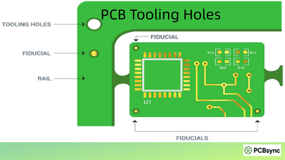
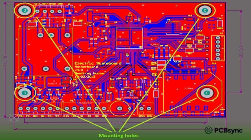
PCB Tooling Holes vs. Mounting Holes vs. Fiducial Markers
I see engineers confuse these three features all the time. Let me clear this up once and for all:
Feature
Purpose
Plating
Location
Typical Size
Tooling Holes
Manufacturing alignment & fixturing
Non-plated
Panel rails/corners
1mm – 3mm
Mounting Holes
Secure finished PCB to enclosure
Plated or non-plated
On the PCB itself
2.5mm – 4.5mm
Fiducial Markers
Optical reference for pick-and-place
Copper pad (no hole)
PCB corners
1mm – 3mm diameter
Tooling holes are temporary—they exist only during pcb manufacturing. Once the panel is depanelized, they’re gone with the breakaway rails.
Mounting holes are permanent. They’re part of your finished product and let you screw the PCB into an enclosure or attach standoffs.
Fiducial markers aren’t holes at all—they’re exposed copper circles that optical systems use to calibrate component placement. You need both fiducials AND tooling holes for proper SMT assembly.
Standard PCB Tooling Hole Sizes
Most manufacturers accept the following standard tooling hole diameters:
Hole Size
Common Use
Notes
1.0mm (39.4 mil)
Small panels, compact designs
Minimum recommended size
1.152mm (45.4 mil)
JLCPCB standard
Required for JLCPCB assembly orders
1.5mm (59 mil)
General purpose
Common industry standard
2.0mm (78.7 mil)
Larger panels
PCBWay recommended size
2.5mm – 3.0mm
Heavy-duty fixturing
For larger boards or test fixtures
3.175mm (0.125″)
US standard
Common in North American facilities
Pro tip: Stick with one consistent size for all tooling holes on your panel. Mixing sizes creates problems with tooling fixtures and increases the chance of assembly errors.
For JLCPCB specifically, their assembly service requires:
Diameter: 1.152mm (45.4 mil)
Type: Non-plated through-hole (NPTH)
Solder mask expansion: 0.148mm
If you’re using PCBWay or other manufacturers, 2.0mm non-plated holes are typically the standard.
The three holes form an “L” pattern. Notice the bottom-left hole is offset—this tells the assembly machine which way is “up.”
PCB Tooling Hole Design Specifications
Getting the specifications right prevents manufacturing delays. Here’s what you need to nail:
Plating Requirements
Always use non-plated (NPTH) holes for tooling. Here’s why:
Non-plated holes have tighter dimensional accuracy
Plating adds copper that can vary in thickness
Plated holes may not fit standard tooling pins
Cost savings—no extra plating step required
Solder Mask Considerations
Your solder mask opening should be larger than the hole diameter. This prevents:
Solder mask from partially covering the hole
Debris accumulation around the hole edge
Interference with tooling pins
A solder mask expansion of 0.1mm – 0.15mm around the hole works well.
Multi-Layer PCB Requirements
For multi-layer boards, you need isolation rings on inner negative layers. Without these, your tooling holes might accidentally connect to power or ground planes.
Layer Type
Requirement
Outer layers
No copper pad (bare hole)
Inner positive layers
No copper around hole
Inner negative layers
Isolation ring required
The isolation ring should be at least 0.3mm (12 mil) larger than the hole diameter.
How to Add PCB Tooling Holes in Popular Design Tools
Here’s how to create tooling holes in the CAD software you’re likely using:
Different manufacturers have different standards. Here’s a quick reference:
Manufacturer
Hole Size
Solder Mask Expansion
Notes
JLCPCB
1.152mm (45.4 mil)
0.148mm
Required for assembly orders
PCBWay
2.0mm
Standard
Non-plated through-holes
Seeed Studio
1.5mm – 2.0mm
Standard
Check panel requirements
AllPCB
1.0mm – 1.5mm
Standard
Verify before ordering
OSH Park
N/A
N/A
They handle panelization
Important: When in doubt, let your manufacturer add the tooling holes. Most fabs offer this as a standard service (sometimes at a small additional cost). They know exactly what their equipment requires.
A minimum of two tooling holes is required for basic X/Y alignment. However, I strongly recommend three holes arranged in an asymmetric “L” pattern. The third hole prevents the board from being loaded backwards (rotated 180°). For larger panels (over 300mm), consider adding a fourth hole for additional stability.
What is the difference between tooling holes and via holes?
Vias are small, plated holes that provide electrical connections between PCB layers—they’re part of your circuit. Tooling holes are larger, non-plated holes used purely for mechanical alignment during manufacturing. Vias carry current; tooling holes hold your board in place. Never confuse the two in your drill files, or you’ll have serious problems.
Can I use existing mounting holes as tooling holes?
Sometimes, but it’s not ideal. Mounting holes are designed for your final product assembly and may be plated for grounding purposes. Tooling holes should be non-plated for accuracy and are typically located on breakaway rails that get removed after manufacturing. If your board has no rails and you’re doing single-unit production, your manufacturer might use mounting holes as tooling references—but check with them first.
Do I need tooling holes if I’m only ordering bare PCBs (no assembly)?
For fabrication-only orders, tooling holes are less critical since you’re not running through pick-and-place machines. However, they still help during drilling and testing. Many manufacturers will add their own tooling to the panel for fabrication. If you’re ordering assembly services (PCBA), tooling holes are essential.
My manufacturer says they’ll add tooling holes automatically. Should I still include them in my design?
It depends on your needs. If you let the manufacturer add them, you have less control over placement—they might end up in inconvenient spots or add breakaway rails you didn’t plan for. If you’re space-constrained or have specific fixture requirements, add your own tooling holes in the locations you want. Most manufacturers accept customer-placed tooling holes as long as they meet their specifications.
Wrapping Up
PCB tooling holes might be the most overlooked feature in board design, but getting them right can save you weeks of manufacturing delays and costly rework. Remember the key points:
Use non-plated holes (NPTH) at standard sizes (1.0mm, 1.5mm, or 2.0mm)
Place them on breakaway rails, not on your finished board
Use three holes in an asymmetric pattern for proper alignment and orientation
Check your manufacturer’s requirements before finalizing—JLCPCB wants 1.152mm, others may differ
Maintain adequate clearance from copper, traces, and the board edge (minimum 3-5mm)
Take five minutes to verify your tooling holes before you hit “Order.” Your manufacturing team—and your schedule—will thank you.
Inquire: Call 0086-755-23203480, or reach out via the form below/your sales contact to discuss our design, manufacturing, and assembly capabilities.
Quote: Email your PCB files to Sales@pcbsync.com (Preferred for large files) or submit online. We will contact you promptly. Please ensure your email is correct.
Notes: For PCB fabrication, we require PCB design file in Gerber RS-274X format (most preferred), *.PCB/DDB (Protel, inform your program version) format or *.BRD (Eagle) format. For PCB assembly, we require PCB design file in above mentioned format, drilling file and BOM. Click to download BOM template To avoid file missing, please include all files into one folder and compress it into .zip or .rar format.


