Inquire: Call 0086-755-23203480, or reach out via the form below/your sales contact to discuss our design, manufacturing, and assembly capabilities.
Quote: Email your PCB files to Sales@pcbsync.com (Preferred for large files) or submit online. We will contact you promptly. Please ensure your email is correct.
Notes: For PCB fabrication, we require PCB design file in Gerber RS-274X format (most preferred), *.PCB/DDB (Protel, inform your program version) format or *.BRD (Eagle) format. For PCB assembly, we require PCB design file in above mentioned format, drilling file and BOM. Click to download BOM template To avoid file missing, please include all files into one folder and compress it into .zip or .rar format.
If you’ve ever had a PCB come back from assembly with mysterious failures that took hours to track down, you know exactly why test points matter. I’ve been there—staring at a board under the microscope, wishing I had just added a few more accessible points during the design phase. The truth is, PCB test points aren’t just nice to have; they’re the difference between catching defects in seconds versus spending days troubleshooting in the lab.
In this guide, I’ll walk you through everything I’ve learned about designing test points for both In-Circuit Testing (ICT) and Flying Probe Testing. Whether you’re working on a prototype or gearing up for high-volume production, getting your test point strategy right from the start will save you countless headaches down the road.
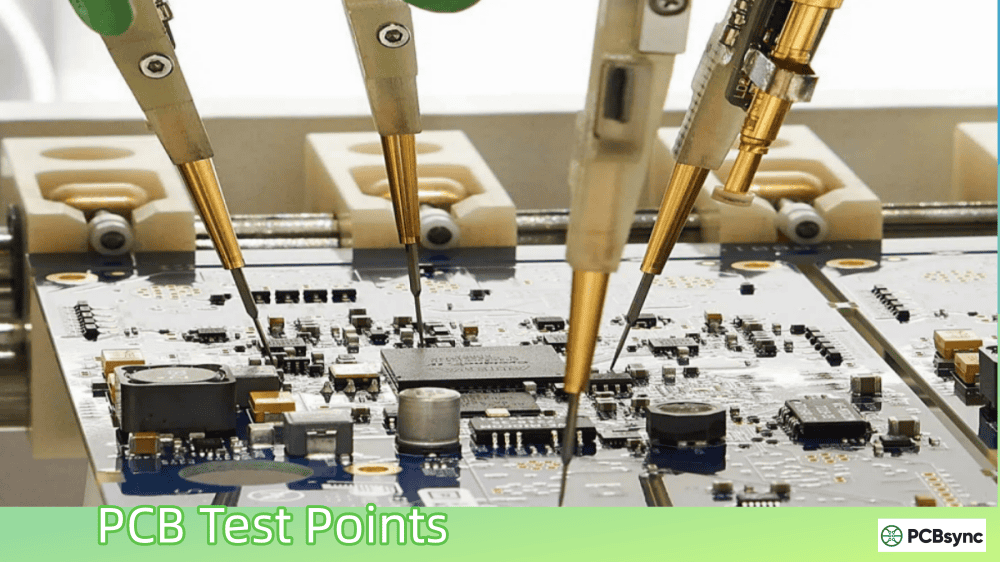
A PCB test point is simply an exposed metal pad on the outer layer of your board that connects to a net in your circuit. Think of it as a designated “access point” where automated test equipment (ATE) can make contact with your circuit to verify that everything is working correctly.
During my first few years as a PCB designer, I treated test points as an afterthought—something to squeeze in after placement and routing were done. That approach cost me dearly. Boards would fail ICT, and we’d discover that critical nets had no probe access. Reworking a nearly-complete layout to add test points is painful, expensive, and often results in compromises.
Here’s what proper test point design gets you:
Early defect detection — Catches shorts, opens, and wrong component values before functional testing
Faster debugging — When something goes wrong, you have direct access to critical signals
Lower production costs — Finding a $0.02 resistor soldering defect beats shipping a failed product
Improved yield — Consistent testing means consistent quality
Understanding ICT vs. Flying Probe Testing
Before diving into design guidelines, you need to understand the two main automated test methods your test points will serve. Each has different requirements, and your production volume will largely determine which one makes sense.
In-Circuit Testing (ICT)
ICT uses a custom “bed of nails” fixture with spring-loaded probes that contact every test point simultaneously. When the board is pressed onto the fixture, all nets are tested in parallel—making it incredibly fast (often under 60 seconds per board).
The catch? That custom fixture is expensive. For a moderately complex board, you’re looking at $5,000 to $25,000 or more for the fixture alone, plus several weeks of development time. Any significant design change means modifying or rebuilding the fixture.
Flying Probe Testing
Flying probe systems use 2-6 movable probes that “fly” around the board, contacting test points sequentially. No custom fixture required—the machine runs directly from your CAD data.
The trade-off is speed. Testing each point individually means cycle times of 5-15 minutes per board, compared to seconds for ICT. That’s fine for prototypes and low-volume runs, but it becomes a bottleneck at scale.
Flying probe does have some advantages beyond cost. It can handle larger boards than most ICT fixtures, and modern systems include optical inspection capabilities that add another layer of defect detection. Some flying probe systems can also perform limited powered functional testing, though not as extensively as dedicated ICT systems.
ICT vs. Flying Probe: Quick Comparison
Factor
ICT (Bed of Nails)
Flying Probe
Setup Cost
$5,000-$25,000+ for fixture
Minimal (programming only)
Setup Time
4-6 weeks
Less than 1 week
Test Speed
30-60 seconds
5-15 minutes
Best For
High volume (10,000+ units)
Prototypes, low volume
Design Changes
Expensive fixture modifications
Simple program update
Test Coverage
Excellent (all points simultaneous)
Excellent (sequential)
Minimum Test Point Size
0.035″ (50 mil preferred)
0.025″ possible
Minimum Spacing
0.100″ center-to-center
0.050″ possible
Many manufacturers use both: flying probe during prototyping and early production, then transition to ICT once the design is stable and volumes justify the fixture investment.
Now let’s get into the specifics. These guidelines come from years of working with contract manufacturers and watching boards pass—or fail—through their test systems.
Test Point Size Requirements
Bigger is better when it comes to test points. Larger pads mean more reliable probe contact and less wear on the test fixture over time.
Test Point Size
Recommendation
Notes
0.050″ (1.27mm)
Ideal
Best probe contact, most reliable
0.040″ (1.02mm)
Good
Standard for most designs
0.035″ (0.89mm)
Acceptable
Minimum for ICT fixtures
0.025″ (0.64mm)
Flying probe only
Too small for reliable ICT
For ICT, I always aim for 0.040″ minimum and 0.050″ where space permits. Square pads offer slightly more surface area than round pads and visually distinguish test points from standard vias in your layout.
Test Point Spacing Guidelines
The spacing between test points determines what size probes your fixture can use. Larger probes are more durable and reliable, but they need room to operate.
Center-to-Center Spacing
Probe Size
Reliability
0.100″ (2.54mm)
100 mil
Highest reliability, lowest fixture cost
0.075″ (1.91mm)
75 mil
Good balance for moderate density
0.050″ (1.27mm)
50 mil
High-density designs, higher fixture cost
Below 0.050″
Micro probes
Flying probe preferred
Critical Placement Rules
These rules have saved me from countless DFM issues:
Keep test points on one side. Ideally, all test points should be on the bottom (solder side) of your PCB. Dual-sided fixtures are expensive and add complexity. If you absolutely must have top-side test points, limit them to non-critical nets.
Maintain edge clearance. Keep test points at least 0.125″ (3.175mm) from the PCB edge. The fixture needs room for tooling pins and board guides.
Avoid component shadows. Tall components on the opposite side of the board can prevent the fixture from applying enough pressure for reliable probe contact. Create a “keep-out zone” under components taller than 0.25″.
Distribute test points evenly. Clustering test points in one area creates stress concentration when the fixture applies pressure. Spread them across the board for more uniform pressure distribution.
Don’t forget power and ground. Every power rail and ground plane needs multiple test points—not just one. This improves noise immunity during testing and gives you redundancy if one probe makes poor contact.
Test Point Assignment Strategy
Here’s the approach I follow for every design:
Start at the schematic level — Flag critical nets for test point access before you even start layout
Assign test points to existing vias first — Why add extra features when you already have accessible points?
Add dedicated pads where needed — For nets with no convenient via access
Prioritize these nets:
Power rails and ground returns
Clock signals
Reset and configuration pins
Communication buses (SPI, I2C, UART)
High-speed differential pairs (at their endpoints)
Any net connected to a high-risk component (fine-pitch BGA, QFN, etc.)
Test Point Design for High-Density PCBs
Modern designs with HDI structures and fine-pitch components present unique challenges. As board density increases, finding space for test points becomes increasingly difficult—but testing becomes even more critical because there are more potential failure points.
The key is strategic planning. You cannot add test points as an afterthought on a high-density board; there simply won’t be room. Instead, test point locations must be considered during component placement, and routing must work around them.
Working with BGA Components
Ball Grid Array packages are notorious for test access problems. Most of the signals disappear under the component where no probe can reach them.
For BGAs, I use these strategies:
Add test vias during fanout — As you route escape traces from the BGA, place test-point-designated vias along critical nets
Use buried vias carefully — If a net only has buried via access, it cannot be tested with ICT or flying probe
Consider boundary scan — For large BGAs, JTAG boundary scan can test connections that probes can’t reach
Microvia Considerations
Be careful when using microvias as test points. The copper plating on microvias is thinner than standard through-hole vias, and aggressive probing can punch through the pad and short to internal layers. Discuss probe force specifications with your test house before committing to microvia test points.
HDI Layer Stack Strategies
For HDI boards with multiple via types, establish a clear hierarchy:
Through-hole vias — Best for test points (full copper plating)
Blind vias to outer layers — Acceptable with appropriate pad size
Buried vias — No probe access, must use alternative testing
Stacked/staggered microvias — Evaluate on a case-by-case basis
Common PCB Test Point Mistakes to Avoid
I’ve made most of these mistakes at some point. Learn from my pain:
Mistake #1: Treating test points as an afterthought
If you wait until routing is complete to think about test points, you’ll be cramming them into whatever space is left. Start planning test access during placement.
Mistake #2: Covering test points with solder mask
This sounds obvious, but I’ve seen it happen. Test points must have exposed copper with solder mask clearance. Double-check your mask layer before sending files to fab.
Mistake #3: Placing test points under components
A test point that’s covered by a connector or heat sink is useless. Verify that all test points remain accessible after assembly.
Mistake #4: Ignoring fixture repeatability
A test point that works fine once might fail intermittently if the probe contact isn’t consistent. Use recommended pad sizes and maintain proper tooling hole placement for fixture alignment.
Mistake #5: No documentation
Your test house needs accurate test point data to build fixtures and write programs. Export test point reports from your CAD system and include them in your manufacturing documentation package.
Test Point Documentation Requirements
When you hand off your design for manufacturing and test, include these items:
Centroid file — X/Y coordinates and net assignments for all test points
Test point report — Generated from your CAD system, listing each test point with its net name, side, and coordinates
Board outline with tooling holes — Critical for fixture design
Component height data — Helps fixture designers plan probe access
Notes on any special requirements — Powered testing, maximum probe force for sensitive components, etc.
Most PCB design tools (Altium Designer, Cadence Allegro, KiCad) have dedicated test point management features that can generate these outputs automatically.
Setting Up Test Points in PCB Design Software
While the specific steps vary by tool, here’s the general workflow:
Define test point design rules — Minimum size, spacing, clearances
Set up test point styles — Templates for different test point types (via-based, pad-based, component-based)
Run automatic assignment — Let the tool place test points on available vias and pads
Review and refine — Check accessibility, add manual test points where needed
Run DRC — Verify spacing and clearance compliance
Generate outputs — Create test point reports for your manufacturer
Useful Resources for PCB Test Point Design
Here are resources I reference regularly:
IPC Standards
IPC-2221 — Generic Standard on Printed Board Design (includes testability guidelines)
IPC-9252 — Guidelines and Requirements for Electrical Testing of Unpopulated Printed Boards
IPC-D-356 — Standard format for test point data exchange
The practical minimum is 0.035″ (0.89mm), but 0.040-0.050″ (1.0-1.27mm) is recommended for reliable probe contact. Smaller test points increase fixture costs and reduce long-term reliability due to probe wear. If your design is extremely space-constrained and you must use 0.035″ pads, discuss this with your test house early—they may need to use specialized probes that increase fixture cost.
Do I need test points for prototypes?
For prototypes, you may not need formal ICT/flying probe test points if you’re doing manual debug. However, adding accessible probe points on critical nets (power rails, clocks, communication buses) will make troubleshooting much easier. It’s good practice to design for testability from the start, because retrofitting test points into a production layout is always harder than including them from the beginning.
How many test points should I have per net?
Generally, one test point per net is sufficient for basic continuity and shorts testing. However, power and ground nets should have multiple test points distributed across the board—I typically add one ground test point for every 10-15 signal test points. For low-value resistors (under 10 ohms), your test engineer may request test points on both sides of the component to get accurate measurements despite probe resistance.
Can I use vias as test points?
Absolutely. Using existing vias as test points is efficient and saves board space. Just ensure the via pad size meets your minimum test point requirements (typically 0.035″ or larger) and that the via isn’t covered by solder mask or tented. Many designers convert the pad shape from round to square when designating a via as a test point—this makes them visually distinct and provides slightly more probe contact area.
What’s the difference between test points and probe points?
Test points are typically automated—they’re designed for ICT or flying probe access. Probe points (or debug points) are for manual testing with handheld probes, often with larger pads, loops, or turret posts for easy clip attachment. Many designs include both types. Probe points usually include silkscreen labels identifying the net name or function for easy reference during debug.
Should test points be masked or unmasked?
Test points must be unmasked (exposed copper) for probe contact. However, you have options for the surface finish. HASL, ENIG, and OSP finishes all work for testing, though some contract manufacturers prefer specific finishes for optimal probe contact. If you’re using OSP finish and your boards will also go through wave soldering, discuss this with your test house—the combination can sometimes cause probe contact issues.
How do I handle testing for boards with components on both sides?
Double-sided assembly makes testing more challenging because tall components on one side can interfere with probe access on the other. The best approach is to concentrate test points on one side (typically the side with fewer tall components) and design keep-out zones on the opposite side. If you must have test points on both sides, expect higher fixture costs and discuss probe access early with your test house.
Wrapping Up
Getting PCB test points right isn’t glamorous work, but it pays off every time a board goes through production. The key is thinking about testability from the start of your design, not as a checkbox at the end.
If you’re designing for high-volume production, invest the effort in proper ICT-compatible test point layout—it’ll pay for itself many times over in reduced defect escapes and faster line throughput. For prototypes and low-volume work, flying probe gives you flexibility without the fixture investment, but you’ll still benefit from well-planned test access.
The best test point layout is one that catches defects before they become problems. Take the time to do it right, and your PCB manufacturing partners (and your customers) will thank you.
Inquire: Call 0086-755-23203480, or reach out via the form below/your sales contact to discuss our design, manufacturing, and assembly capabilities.
Quote: Email your PCB files to Sales@pcbsync.com (Preferred for large files) or submit online. We will contact you promptly. Please ensure your email is correct.
Notes: For PCB fabrication, we require PCB design file in Gerber RS-274X format (most preferred), *.PCB/DDB (Protel, inform your program version) format or *.BRD (Eagle) format. For PCB assembly, we require PCB design file in above mentioned format, drilling file and BOM. Click to download BOM template To avoid file missing, please include all files into one folder and compress it into .zip or .rar format.


