Inquire: Call 0086-755-23203480, or reach out via the form below/your sales contact to discuss our design, manufacturing, and assembly capabilities.
Quote: Email your PCB files to Sales@pcbsync.com (Preferred for large files) or submit online. We will contact you promptly. Please ensure your email is correct.
Notes: For PCB fabrication, we require PCB design file in Gerber RS-274X format (most preferred), *.PCB/DDB (Protel, inform your program version) format or *.BRD (Eagle) format. For PCB assembly, we require PCB design file in above mentioned format, drilling file and BOM. Click to download BOM template To avoid file missing, please include all files into one folder and compress it into .zip or .rar format.
If you’ve ever tried hand-soldering a board full of 0402 resistors or a fine-pitch QFP, you know the pain. Your hands shake, the flux fumes get to you, and three hours later you’re still fixing bridges. That’s exactly why PCB stencils exist—and why getting them right matters so much.
I’ve been working with SMT assembly for over a decade now, and I can tell you that the stencil is often the most underestimated part of the entire process. Get it wrong, and you’ll spend your days chasing tombstones and solder bridges. Get it right, and boards practically assemble themselves.
This guide covers everything you need to know about PCB stencils—from choosing the right type and thickness to actually using them without messing up your paste deposit. Whether you’re prototyping in your garage or running a production line, the principles here will save you headaches.
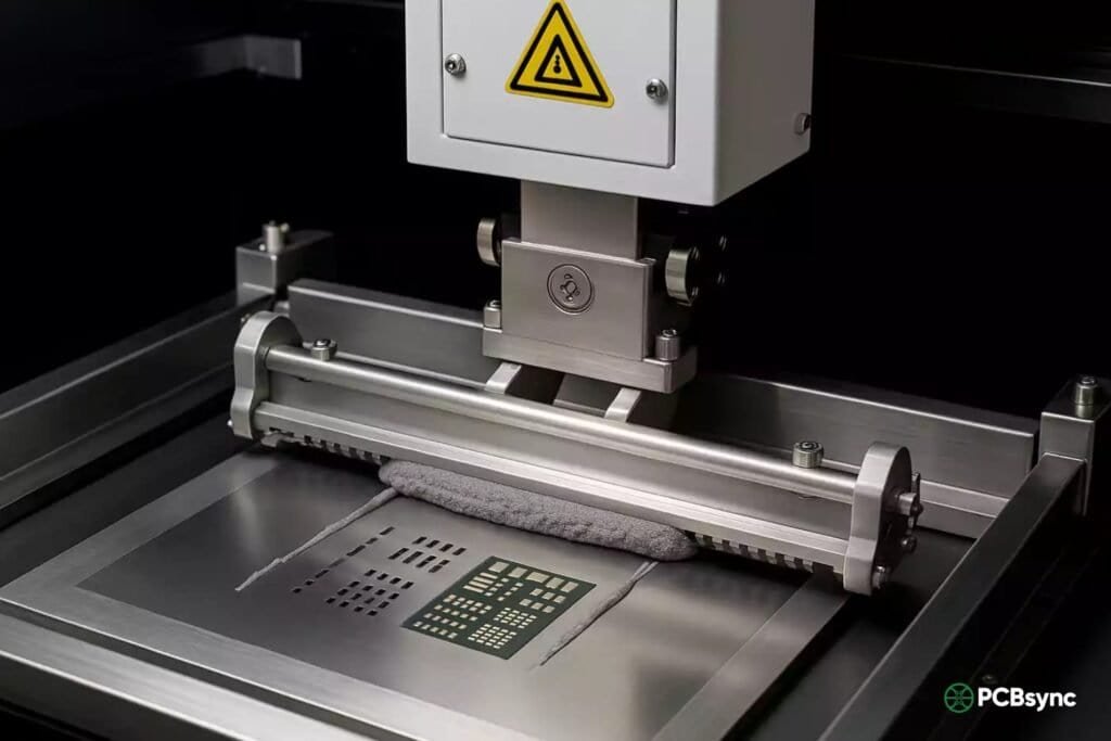
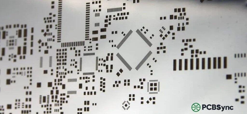
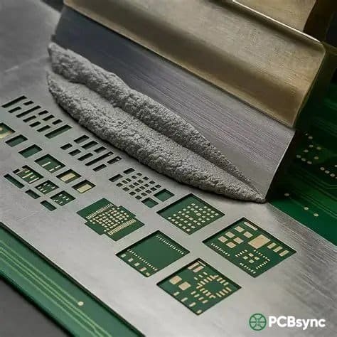
A PCB stencil (also called an SMT stencil or solder paste stencil) is a thin sheet of material—usually stainless steel—with precisely cut openings that match the solder pads on your circuit board. You place the stencil on top of your bare PCB, squeegee solder paste across it, and the paste deposits only where you need it: right on the pads.
Simple concept, massive impact.
The stencil’s job is to deposit the exact right amount of solder paste in exactly the right places. Too much paste and you get bridging between adjacent pins. Too little and you end up with cold joints or open circuits. The precision required here is surprisingly tight—we’re often talking about controlling paste volumes down to fractions of a cubic millimeter.
Choose the stencil type that best fits your production requirements.
Framed Stencil
Permanently mounted in aluminum frame. Best for high-volume production with automated printing equipment.
High VolumeAutomatedReusable
Frameless Stencil
Flexible sheet without frame. Used with universal frame systems. Ideal for cost-effective prototyping.
PrototypeLow CostFlexible
Prototype Stencil
Quick-turn stencil for R&D and small batch assembly. Usually frameless with faster delivery.
Quick TurnR&DSmall Batch
Step Stencil
Multiple thickness levels for mixed component heights. Perfect for boards with varied paste requirements.
Multi-LevelComplex PCBMixed Components
Electroformed Stencil
Nickel electroforming for ultra-fine pitch. Superior aperture walls for 0201 and 01005 components.
Ultra Fine PitchNickelPremium
Nano-Coated Stencil
Special coating for improved paste release and longer cleaning intervals. Reduces bridging defects.
Anti-BridgingEasy CleanEnhanced
📋 Stencil Type Recommendation
Aperture Design Calculator
Component land pad width
Component land pad length
Typical: 0.10 – 0.15mm
Typical: 5-15% reduction
💡Area Ratio Rule: For reliable paste release, maintain Area Ratio ≥ 0.66 (IPC recommendation). Higher ratios result in better paste transfer.
📐 Aperture Calculation Results
Aperture Width
—
Aperture Length
—
Aperture Area
—
Wall Area
—
Area Ratio
—
Aspect Ratio
—
Area Ratio Assessment
0.3 (Poor)0.50.66 (Min)0.81.0+ (Excellent)
Area Ratio is within acceptable range
Stencil Cost Estimator
💰 Cost Estimate Breakdown
Base Stencil Price$0.00
Size Premium$0.00
Material Premium$0.00
Additional Options$0.00
Lead Time Adjustment$0.00
Quantity (1 pcs)$0.00
Estimated Total$0.00
* Prices are estimates only. Actual costs may vary based on design complexity and supplier.
Stencil Thickness Selection Guide
Select the appropriate stencil thickness based on your smallest component pitch and aperture size.
Component Type
Pitch (mm)
Recommended Thickness
Notes
01005 / 0201
0.15 – 0.25
0.08mm (3mil)
Ultra-fine pitch, electroformed recommended
0402 / Fine Pitch QFP
0.30 – 0.40
0.10mm (4mil)
Fine pitch applications
0603 / Standard QFP
0.50
0.12mm (5mil)
Most common thickness
0805 / SOT / BGA
0.65 – 0.80
0.12 – 0.15mm
Standard SMT assembly
1206 / Large Chip
1.00+
0.15mm (6mil)
Large components, connectors
Through-Hole / Shield
2.54+
0.20mm (8mil)
Maximum paste deposit
⚠️Mixed Components: When your PCB has both fine-pitch and large components, consider using a Step Stencil with multiple thickness levels, or select the thickness based on your finest pitch components.
Quick Thickness Calculator
Recommended Thickness
—
Max Thickness
—
PCB Stencil Design Best Practices
1
Maintain Proper Area Ratio (≥0.66)
The area ratio (aperture area ÷ wall area) should be at least 0.66 for reliable paste release. For fine-pitch components, aim for 0.70 or higher. Use the aperture calculator to verify your design.
2
Apply Aperture Reduction for QFP/QFN
Reduce aperture size by 5-15% compared to pad size for QFP/QFN packages to prevent solder bridging. Use 1:1 ratio for passive components like 0402 and 0603.
3
Use Home Plate or D-Shape Apertures for BGA
For BGA components, consider using home plate, D-shape, or square apertures with corner radius instead of round. This increases paste volume while maintaining proper release.
4
Account for Paste Volume on Thermal Pads
Large thermal pads should use windowed or crosshatched aperture patterns (typically 50-75% coverage) to prevent voiding and component floating during reflow.
5
Select Appropriate Stencil Thickness
Match stencil thickness to your finest pitch component. Use the aspect ratio rule: aperture width should be ≥1.5× stencil thickness for reliable paste release.
6
Include Fiducial Marks
Add at least 2-3 fiducial apertures matching your PCB fiducials for accurate stencil-to-board alignment, especially for fine-pitch components.
7
Consider Electropolish or Nano Coating
For fine-pitch applications, electropolished or nano-coated stencils provide smoother aperture walls, improving paste release and reducing cleaning frequency.
8
Verify Gerber Files Before Ordering
Always use paste layer (cream layer) Gerber files for stencil fabrication, not solder mask or copper layers. Verify aperture locations match your PCB design.
Common Stencil Design Issues
🔴 Solder Bridging
Too much paste between fine-pitch leads causes shorts.
That first step—the paste print—determines roughly 60-70% of your final assembly quality. A bad print propagates through the entire process. This is why stencil design and selection isn't just a checkbox item; it's a critical engineering decision.
Types of PCB Stencils: Choosing the Right One
Not all stencils are created equal. The type you need depends on your production volume, component pitch, and budget. Here's a breakdown of what's available:
Laser-Cut PCB Stencils
This is the industry standard and probably what you should be using for most applications. A high-powered laser cuts apertures directly into stainless steel foil, creating clean, precise openings with smooth walls.
Best for: General SMT assembly, prototypes, medium-to-high volume production
Advantages:
Excellent precision (±0.001" tolerance typical)
Smooth aperture walls for good paste release
Fast turnaround from most suppliers
Cost-effective for most applications
Limitations:
Aperture walls can have slight taper from the laser cutting process
May need electropolishing for ultra-fine pitch applications
Electroformed PCB Stencils
These are the premium option. Instead of cutting material away, electroformed stencils are built up atom-by-atom using an electroplating process. The result is apertures with naturally smooth, slightly trapezoidal walls that release paste beautifully.
Best for: Fine-pitch components (0.4mm pitch and below), BGAs, µBGAs, flip-chip applications
Advantages:
Superior paste release due to smooth trapezoidal walls
Nickel construction is harder than stainless steel
Lower coefficient of friction improves paste transfer
Best choice for challenging ultra-fine pitch designs
Limitations:
Approximately 50% more expensive than laser-cut stencils
Longer lead times
Chemically Etched PCB Stencils
An older technology where photoresist and acid etch the apertures from both sides of the foil. This creates an "hourglass" shaped aperture wall.
Best for: Very thick stencils, simple designs with large apertures
Advantages:
Lower cost for simple applications
Good for adhesive dispensing stencils
Limitations:
Poor aperture wall quality
Hourglass shape causes inconsistent paste release
Not suitable for fine-pitch components
Generally being phased out in favor of laser cutting
Framed vs. Frameless PCB Stencils
Beyond manufacturing method, stencils come in two mounting configurations:
Feature
Framed Stencil
Frameless Stencil
Construction
Foil permanently glued into aluminum frame
Loose foil used with tensioning system
Best for
High-volume production
Prototypes, low volume
Cost
Higher initial cost
Lower cost per stencil
Storage
Requires more space
Easy to store flat
Durability
Very robust
Requires careful handling
Compatibility
Works with most stencil printers
Needs compatible frame system
For prototype work, frameless stencils make sense economically. For production, framed stencils deliver more consistent results over thousands of print cycles.
Step Stencils for Mixed Component Boards
Here's where things get interesting. Modern PCBs often mix fine-pitch ICs (needing thin stencils) with large connectors or RF shields (needing thick stencils for more paste). A step stencil solves this by having different thickness zones on a single foil.
Step-down areas: Material removed to create thinner regions for fine-pitch components
Step-up areas: Material added to create thicker regions for components needing more solder (like connectors or pin-in-paste through-holes)
The catch is that steps need adequate "keep-out" distance from nearby apertures—typically 35 mils per mil of step height. For boards where fine-pitch and large components are close together, you might need a two-print stencil approach instead.
PCB Stencil Thickness: The Critical Parameter
If there's one thing that trips up engineers new to stencil design, it's thickness selection. The stencil thickness directly controls how much paste you deposit, and the relationship isn't always intuitive.
How Stencil Thickness Affects Paste Volume
Thicker stencil = more paste volume (taller brick of paste) Thinner stencil = less paste volume (shorter brick of paste)
But it's not just about "more" or "less." You need the right amount for each component type. Too much paste on a 0402 chip causes bridging. Too little paste under a large QFN thermal pad causes voids and poor heat dissipation.
Stencil Thickness Selection Guide
Here's a practical reference table based on IPC-7525 guidelines and real-world experience:
Component Type
Pitch
Recommended Thickness
0201 chip components
N/A
0.08mm (3 mil)
0402 chip components
N/A
0.10mm (4 mil)
0603 chip components
N/A
0.10-0.12mm (4-5 mil)
Fine-pitch QFP
≤0.5mm
0.10-0.12mm (4-5 mil)
Standard QFP
>0.5mm
0.12-0.15mm (5-6 mil)
µBGA/CSP
0.3-0.4mm
0.08-0.10mm (3-4 mil)
BGA
0.5-1.0mm
0.12-0.13mm (5 mil)
BGA
>1.0mm
0.15mm (6 mil)
Standard SMD
General
0.12-0.15mm (5-6 mil)
Connectors, large parts
N/A
0.15-0.20mm (6-8 mil)
The golden rule: Let your smallest, finest-pitch component dictate the stencil thickness. If you have a mix of component sizes, you may need a step stencil or aperture modifications to compensate.
Area Ratio and Aspect Ratio: The Technical Side
Two ratios govern whether paste will release cleanly from your stencil apertures:
Aspect Ratio = Aperture Width ÷ Stencil Thickness
The minimum acceptable aspect ratio is 1.5. Below this, paste tends to stick in the aperture rather than transferring to the pad.
Area Ratio = Aperture Area ÷ Aperture Wall Area
For rectangular apertures: Area Ratio = (L × W) ÷ (2 × (L + W) × T)
The minimum acceptable area ratio is 0.66. For better performance, aim for >0.66.
What this means practically: as your apertures get smaller (for fine-pitch components), you need thinner stencils to maintain acceptable ratios. A 0.3mm aperture on a 0.15mm thick stencil won't print well—the area ratio is too low and paste won't release.
PCB Stencil Aperture Design Principles
The aperture (the hole in your stencil) isn't just a copy of your pad shape. Good aperture design requires deliberate modifications to ensure clean paste transfer and prevent defects.
Aperture Size Relative to Pad Size
A common starting point: make apertures slightly smaller than pads.
Solder Type
Typical Aperture Reduction
Lead-free
1:1 ratio (same as pad) or slight reduction
Leaded (SnPb)
2 mil (0.05mm) reduction per side
Fine-pitch (<0.5mm)
10-20% reduction from pad size
BGA (pitch >1.0mm)
1:1 ratio
BGA (pitch 0.5-1.0mm)
10-15% reduction
The slight reduction serves two purposes: it prevents paste from squeezing out beyond the pad edges, and it creates a better gasket seal between stencil and PCB during printing.
Aperture Shapes and Their Effects
Different shapes affect paste transfer efficiency:
Rectangular/Square: Standard choice for most SMD components
Circular: Common for BGA balls; matches the spherical solder joint shape
Rounded corners: Improves paste release by eliminating sharp corners where paste can stick
"Squircle": A square with rounded corners—actually provides the best paste transfer efficiency according to research
Home-plate: Pentagon shape used to reduce mid-chip solder balls on chip components
Bow-tie/Dog-bone: Used for QFN center pads to reduce voiding
Special Aperture Designs for Common Components
QFN/DFN Thermal Pads: Large center pads under QFNs need special treatment. A solid aperture deposits too much paste, causing the component to float and tilt during reflow. Instead, use a "window pane" or grid pattern that covers 50-75% of the pad area. If vias are in the thermal pad, position stencil webbing over the vias to prevent paste from wicking down.
BGA Apertures: For BGAs, circular apertures matching the ball diameter work well. Reduce aperture size by 10-15% for pitches below 0.5mm to prevent bridging during reflow.
Small Chip Components (0402, 0201): These are prone to tombstoning. Keep apertures at 1:1 ratio or with only minimal reduction. Home-plate apertures can help with mid-chip solder balls on 0603 and larger, but actually increase tombstone risk on 0402s and smaller.
How to Use a PCB Stencil: Step-by-Step Process
Having the right stencil is only half the battle. Using it correctly makes the difference between good boards and scrap.
Preparation Before Printing
Solder paste conditioning: Remove paste from refrigeration and let it reach room temperature (typically 2-4 hours). Cold paste doesn't print well. Once at room temp, stir or knead the paste to ensure homogeneous consistency.
PCB inspection: Check that boards are clean, flat, and free from oxidation. OSP-finish boards are particularly sensitive to oxidation—limit exposure time after opening vacuum packaging.
Stencil inspection: Verify the stencil matches your PCB revision. Check for clogged apertures, damage, or residual paste from previous runs. Clean if necessary with isopropyl alcohol and lint-free wipes.
Environment check: Ideal conditions are 22-25°C and 40-60% relative humidity. Extreme conditions affect paste rheology and print quality.
Alignment and Setup
Proper alignment is critical—misaligned paste means misaligned components and potential defects.
Secure the PCB: Use a vacuum fixture or mechanical holders to keep the board stationary. Surrounding spacers should match PCB thickness (typically 1.6mm).
Align the stencil: Use fiducial marks on both the stencil and PCB for precise registration. Most stencil printers use vision systems to automatically align to fiducials. For manual printing, carefully align apertures to pads before fixing the stencil position.
Set stencil gap: The stencil should contact the PCB surface with zero gap during print. Some printers use "off-contact" printing where the stencil lifts after paste deposit—this requires proper snap-off settings.
The Printing Process
Apply paste: Place a bead of solder paste along one edge of the stencil, in front of the squeegee. Use enough paste to maintain a consistent roll in front of the squeegee throughout the stroke.
Squeegee stroke: Apply the squeegee at a 45-60° angle with consistent pressure (typically 0.5-1.5 kg per cm of blade length). Move the squeegee at a steady speed (typically 20-80mm/sec depending on aperture sizes).
Stencil separation: This is crucial. Lift the stencil straight up, slowly and smoothly (1-3mm/sec separation speed). Fast or angled separation pulls paste out of the apertures and causes smearing.
Inspect the print: Examine paste deposits visually or with SPI (Solder Paste Inspection). Look for complete coverage, consistent height, and no bridging or smearing.
Stencil Cleaning and Maintenance
Regular cleaning prevents defects from accumulating:
Underside wipe: Every 5-10 prints, wipe the stencil underside with solvent-dampened wipes to remove paste bleeding through apertures
Full cleaning: After each batch or at end of shift, thoroughly clean both sides of the stencil
Cleaning methods: IPA wipes for light cleaning; ultrasonic cleaning for thorough maintenance
Storage: Store clean, dry stencils flat or in protective bags to prevent damage
Advanced Stencil Technologies: Nano Coatings
For challenging applications, nano-coated stencils offer significant improvements in paste release. These coatings (like NanoProTek or similar products) create a low-surface-energy layer on aperture walls that reduces paste adhesion.
Benefits of nano coatings:
15-30% improvement in paste transfer efficiency
Reduced cleaning frequency
Better performance on low area ratio apertures
Extended stencil life
Considerations:
Adds cost to stencil procurement
Coating may wear over time and need reapplication
Most beneficial for fine-pitch and challenging designs; overkill for standard applications
If you're struggling with paste release on fine-pitch components even with proper thickness selection, nano coating is worth investigating before jumping to electroformed stencils.
Solder Paste Types and PCB Stencil Compatibility
Your stencil doesn't work in isolation—it works with solder paste, and the paste characteristics affect print quality significantly. Understanding this relationship helps you make better decisions.
Solder Paste Particle Sizes
Solder paste is classified by particle size, with each type suited to different aperture sizes:
Type
Particle Size Range
Best For
Type 3
25-45 µm
Standard SMD, apertures >0.25mm
Type 4
20-38 µm
Fine-pitch (0.4-0.5mm), smaller apertures
Type 5
15-25 µm
Ultra-fine pitch, µBGA, apertures <0.2mm
Type 6
5-15 µm
Advanced packaging, <0.15mm apertures
The rule of thumb: At least 5 solder particles should fit across the smallest aperture width. If your aperture is 0.2mm (200µm) wide, Type 4 paste (max 38µm particles) gives you roughly 5 particles across—that's the minimum. Type 5 would be safer.
Using paste that's too coarse for your apertures leads to clogging and inconsistent transfer. Using paste that's unnecessarily fine costs more and offers no benefit.
Lead-Free vs. Leaded Solder Paste Considerations
Lead-free solder pastes (SAC305, SAC405, etc.) behave differently than traditional tin-lead:
Higher surface tension: Lead-free paste is "stickier" and releases from apertures less easily
Higher reflow temperatures: Doesn't directly affect stencil printing, but affects overall process compatibility
Different wetting characteristics: May require aperture modifications compared to leaded paste guidelines
For lead-free processes, many engineers maintain a 1:1 aperture-to-pad ratio rather than reducing apertures, since the paste is less prone to spreading during reflow.
Common PCB Stencil Defects and Solutions
Even with proper technique, issues arise. Here's how to diagnose and fix the most common problems:
Solder Bridging
Symptom: Paste connects adjacent pads, causing shorts after reflow
Causes:
Apertures too large
Stencil too thick for fine-pitch components
Excessive squeegee pressure
Slow separation speed
Paste smearing from dirty stencil underside
Solutions:
Reduce aperture size by 10-15%
Use thinner stencil (try 0.10mm instead of 0.12mm)
Reduce squeegee pressure incrementally
Increase separation speed slightly
Clean stencil underside more frequently
Insufficient Solder (Starved Joints)
Symptom: Not enough paste deposited; weak or open joints after reflow
For ordering stencils, these suppliers offer quality products with reasonable turnaround:
OSH Stencils - Affordable option for hobbyists and prototypes
Stencils Unlimited - Wide range of stencil types including electroformed
PCB Unlimited - Good for prototype stencil kits
JLCPCB/PCBWay - Budget-friendly options often bundled with PCB orders
Seeed Studio Fusion - Another budget option with good quality
Calculators and Tools
Area Ratio Calculator: Many stencil suppliers provide online calculators to verify your aperture designs
Gerber Viewers: Use free tools like Gerbv or KiCad's viewer to verify paste layer data before ordering
Design for Manufacturability: PCB Stencil Considerations
Smart PCB design makes stenciling easier. Here are DFM tips that relate directly to stencil performance:
Pad Design Best Practices
Consistent pad sizes: When possible, use consistent pad geometries to simplify aperture design
Thermal relief on ground planes: Large ground pads connected to copper pours cause uneven heating during reflow, contributing to tombstoning. Use thermal relief patterns.
Avoid vias in pads: If you must have vias in SMD pads (common under QFN thermal pads), use filled and plated-over vias, or design stencil apertures to avoid depositing paste directly into via holes
Adequate pad spacing: The tighter your pad spacing, the thinner your stencil needs to be. Design with stencil limitations in mind.
Component Placement Considerations
Group similar components: Clustering similar-pitched components together makes step stencil design easier if needed
Keep fine-pitch away from edges: Components at board edges are harder to print consistently due to stencil edge effects
Orient polarized components consistently: This doesn't affect stenciling directly, but makes inspection easier
Working with Your Assembly House
If you're sending boards to a contract manufacturer, communicate about stencil requirements:
Ask what stencil thickness they recommend for your design
Provide complete paste layer Gerber files
Discuss any special requirements for QFNs, BGAs, or fine-pitch components
Request they share SPI data so you can correlate any assembly issues with paste print quality
Frequently Asked Questions About PCB Stencils
What files do I need to order a PCB stencil?
You need the Gerber paste layer files (typically named something like *.GTP for top paste or *.GBP for bottom paste). Also provide board outline data and fiducial locations. Most suppliers accept standard Gerber RS-274X format. Some also accept ODB++ or IPC-2581 formats.
Can I reuse a PCB stencil?
Absolutely. With proper cleaning and storage, a quality stainless steel stencil can last for thousands of print cycles. Frameless prototype stencils are more delicate but still good for dozens to hundreds of prints. Always clean stencils before storage to prevent paste residue from hardening in apertures.
What's the difference between a stencil and a screen?
A stencil has apertures cut through a solid foil. A screen (used in screen printing) is a mesh with a patterned emulsion. For SMT solder paste application, stencils are standard because they provide more precise paste volume control than screens.
Do I need a stencil for through-hole components?
Traditional through-hole components are wave soldered, not stenciled. However, "pin-in-paste" or "intrusive reflow" techniques use stencils to apply paste to plated through-holes, allowing through-hole components to be reflow soldered alongside SMT parts. This requires step-up stencils or overprint techniques to deposit enough paste volume.
How do I choose between frameless and framed stencils?
Choose frameless if:
You're prototyping or doing low-volume runs
Budget is constrained
You have a compatible tensioning frame system
Storage space is limited
Choose framed if:
You're running production volumes
Maximum print consistency is required
The stencil will see heavy use
You want the most robust handling
Final Thoughts
Getting your PCB stencil right isn't glamorous work, but it's foundational work. I've seen engineers spend days debugging assembly defects that traced back to a thickness mismatch or an aperture design issue that could have been caught with a five-minute calculation.
The key takeaways:
Match stencil thickness to your smallest/finest component—this drives the whole design
Verify area ratio and aspect ratio for any apertures you're concerned about
Consider step stencils when you have dramatically different paste volume requirements
Technique matters—proper squeegee angle, pressure, and separation speed make a measurable difference
Clean regularly—it's the cheapest defect prevention available
Whether you're building one board or a million, the stencil is where quality assembly starts. Invest the time to get it right, and everything downstream gets easier.
Inquire: Call 0086-755-23203480, or reach out via the form below/your sales contact to discuss our design, manufacturing, and assembly capabilities.
Quote: Email your PCB files to Sales@pcbsync.com (Preferred for large files) or submit online. We will contact you promptly. Please ensure your email is correct.
Notes: For PCB fabrication, we require PCB design file in Gerber RS-274X format (most preferred), *.PCB/DDB (Protel, inform your program version) format or *.BRD (Eagle) format. For PCB assembly, we require PCB design file in above mentioned format, drilling file and BOM. Click to download BOM template To avoid file missing, please include all files into one folder and compress it into .zip or .rar format.


