Inquire: Call 0086-755-23203480, or reach out via the form below/your sales contact to discuss our design, manufacturing, and assembly capabilities.
Quote: Email your PCB files to Sales@pcbsync.com (Preferred for large files) or submit online. We will contact you promptly. Please ensure your email is correct.
Notes: For PCB fabrication, we require PCB design file in Gerber RS-274X format (most preferred), *.PCB/DDB (Protel, inform your program version) format or *.BRD (Eagle) format. For PCB assembly, we require PCB design file in above mentioned format, drilling file and BOM. Click to download BOM template To avoid file missing, please include all files into one folder and compress it into .zip or .rar format.
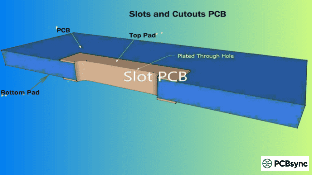
If you’ve ever worked with blade-style connectors or components with rectangular leads, you know that standard round holes just don’t cut it. That’s where PCB slots come in — and getting them right can make the difference between a board that works perfectly and one that ends up in the reject pile.
I’ve seen plenty of designs come back from fabrication with slot issues, usually because the designer didn’t specify them correctly in the Gerber files or mixed up plated and non-plated requirements. This guide covers everything you need to know about PCB slot design, from basic concepts to advanced pcb manufacturing considerations.
A PCB slot is a non-circular hole in a circuit board that’s too large or irregularly shaped to be created using standard drilling methods. Unlike round holes that can be punched through with a drill bit, slots require a routing bit to cut them out during PCB fabrication.
Think of it this way: if a standard via is like punching a hole with a paper punch, a slot is more like cutting with scissors — you’re removing material along a path rather than at a single point.
PCB slots serve several critical functions in modern circuit board design:
Accommodating components with rectangular or blade-style leads
Providing electrical isolation between high-voltage traces
Creating mechanical mounting points
Improving thermal management through airflow channels
Enabling custom board profiles and cutouts
The key distinction is that slots can be either plated (with copper coating for electrical connection) or non-plated (bare FR4 for mechanical or isolation purposes). Choosing the wrong type will cause problems — I’ve seen boards where mounting slots were accidentally plated, creating unintended short circuits.
Types of PCB Slots: Plated vs. Non-Plated
Understanding when to use each type is fundamental to good PCB slot design. Here’s what separates them:
Plated Through Slots (PTS)
Plated slots have copper plating on the inner walls, connecting the top and bottom copper layers — essentially functioning like elongated plated through-holes. They’re the go-to choice when you need electrical connectivity.
When to use plated slots:
Through-hole components with rectangular pins
Large blade-style connectors (USB, HDMI, card-edge)
Components where round holes would waste board space
Multilayer PCBs requiring layer-to-layer connection through the slot
The plating process is identical to standard PTH: the manufacturer mills the slot, performs electroless copper deposition, then electroplates to achieve the required thickness.
Non-Plated Through Slots (NPTH)
Non-plated slots have no copper on the interior walls. They’re purely mechanical features used for isolation or structural purposes.
When to use non-plated slots:
Voltage isolation between high-voltage traces (preventing arc-over)
Thermal management slots for heat dissipation
Mechanical mounting points
Board cutouts and irregular profiles
Cable routing channels
One important note: non-plated slots should have copper pulled back from the slot edge by at least 6 mils (0.15mm) to prevent accidental plating during manufacturing.
Quick Comparison Table: Plated vs Non-Plated PCB Slots
Getting your slot dimensions right is critical — too small and you’ll get manufacturing rejects; too large and you’re wasting board space. Here are the industry-standard specifications:
Minimum PCB Slot Sizes
Parameter
Plated Slots
Non-Plated Slots
Minimum width
0.5mm
0.8mm
Minimum length
1.0mm (or 2× width)
1.6mm (or 2× width)
Inside corner radius
0.5mm minimum
0.5mm minimum
Standard milling tool
2.0mm diameter
2.0mm diameter
Special milling tool
0.8mm – 2.0mm range
0.8mm – 2.0mm range
The 2:1 Length-to-Width Rule
Here’s a rule that trips up a lot of designers: the minimum slot length must be at least 2× the slot width. This isn’t arbitrary — it’s a manufacturing constraint based on how NC milling cutters operate.
For example:
0.5mm wide slot → minimum 1.0mm length
0.6mm wide slot → minimum 1.2mm length
0.8mm wide slot → minimum 1.6mm length
If you specify a slot that violates this rule, expect either a rejection or a conversation with your fab house about what they can actually produce.
Inside Corner Considerations
Because slots are cut with round milling tools, inside corners will always have a radius equal to half the tool diameter. The standard 2.0mm milling tool produces 1.0mm inside corner radii, while the smallest common tool (0.8mm) produces 0.4mm radii.
This matters for enclosure designs — if your slot needs to fit a square-cornered component or mechanical feature, you’ll need to account for these rounded corners in your design or specify a smaller milling tool (which may add cost).
Flex and Rigid-Flex Considerations
For flex and rigid-flex PCBs, the rules change slightly. The thinner material allows for smaller slots, and laser cutting becomes an option:
Always confirm capabilities with your manufacturer, as these vary significantly between fab houses.
How to Design PCB Slots in Your CAD Software
The biggest cause of slot-related manufacturing issues? Improper definition in the design files. Here’s how to get it right:
Defining Slots in Gerber Files
The safest, clearest method is to define slots in the Gerber mechanical layer. This layer shows the PCB profile along with all slots and cutouts, leaving no ambiguity for the manufacturer.
Two approaches work well:
Draw with appropriate line width: Use a 0.5mm line to trace the slot outline. The line center defines the slot edge, and this method makes it easy to visually verify copper clearance to the board edge.
Use flashes or draws: Specify the exact slot dimensions using aperture flashes or draws matching the required slot size.
Critical rules:
Always combine slot definitions with the PCB outline (contour) in the Gerber file
Ensure the mechanical layer aligns with copper layers
Include the PCB outline in the copper layer as well for redundancy
Never define slots only in copper or legend layers — they’re easily overlooked
Using Drill Files for Slot Definition
Some CAD systems allow slots to be defined in the NC drill file using X and Y dimensions (width and length respectively). This can work, but:
Not all systems support this method consistently
Overlapping holes to create slots can cause issues
Some manufacturers prefer separate mechanical layer definition
When using drill file definition, specify the finished slot size — the manufacturer will compensate for plating thickness on plated slots.
The README File Backup
Whenever there’s any potential ambiguity, document your slot requirements in a README file included with your Gerber package. Specifically note:
Which slots are plated vs. non-plated
Any non-standard tolerances required
References to which layer contains slot definitions
Special instructions for complex slot patterns
This 30-second step has saved countless boards from manufacturing errors.
Step-by-Step: Creating PCB Slots in Popular CAD Tools
For plated slots: Create a pad with slot hole definition using Pad Properties
For non-plated slots: Use the mechanical layer or board cutout features
Define slot dimensions in the Properties panel (X and Y for width and length)
Verify slots appear correctly in your Gerber preview before export
Most versions of Altium support native slot definitions. Non-circular plated holes export as board cutouts on Mechanical Layer 1 — ensure you include this layer in your manufacturing output.
KiCad
Open your design in Pcbnew
For slots in component footprints: Define slot shapes on the Edge.Cuts layer
For board cutouts: Draw closed shapes on Edge.Cuts layer
Use View → Drawing Mode → Sketch Pads to verify slot shapes
Note: KiCad handles slots as cutout outlines. While not native “slots” per se, board manufacturers interpret Edge.Cuts geometry correctly in Gerber files.
Eagle (Autodesk Fusion 360)
Open your board layout
For through-hole slots: Use an oblong pad definition matching your slot dimensions
Draw slot outlines using the dimension layer
Note that Eagle’s autorouter won’t route inside pad areas — verify connectivity manually
Limitation: Eagle’s dimension layer approach can cause dimension errors with complex slot matrices. Consider using milling layer definitions for complex designs.
Design Verification Checklist
Before sending files to manufacturing, verify:
Slots appear on mechanical/outline layer
Plated slots have copper pads on top and bottom layers
Non-plated slots have copper pulled back from edges
Inside corners have appropriate radii for milling tools
README file documents any ambiguous slots
Gerber preview shows slots correctly positioned
PCB Slot Manufacturing Process
Understanding how slots are manufactured helps you design better boards. Here’s what happens at the fab house:
Milling Process
Most PCB slots are created through NC (Numeric Controlled) milling, similar to CNC machining. The process uses a rotating grooving cutter bit to remove material along the slot path.
Solution: Design with the expected corner radius in mind. For standard 2.0mm tools, that’s a 1.0mm inside corner radius. If sharper corners are required, specify smaller tooling (and expect potential cost increase).
Mistake 5: Copper Too Close to Non-Plated Slot Edges
Problem: Copper positioned too close to NPTH slot edges may accidentally plate during manufacturing, creating shorts or isolation failures.
Solution: Pull copper back at least 6 mils (0.15mm) from non-plated slot edges — more if your design rules require greater clearance.
Mistake 6: Missing Slot Definitions When Exporting Gerber
Problem: Slots are visible in your CAD tool but don’t make it into the exported Gerber package.
Solution: Always preview Gerber output in a standalone viewer (Gerbv, Altium 365 Viewer, etc.) before submitting. Verify every slot appears correctly.
Applications of PCB Slots in Real Designs
PCB slots aren’t just theoretical — they solve real design challenges across industries:
Connector Mounting
Large blade-style connectors (USB Type-A, HDMI, card-edge connectors) use plated slots to accommodate their rectangular pins. Round holes would waste significant board space and create weaker solder joints.
High-Voltage Isolation
In power electronics, non-plated slots create physical air gaps between high-voltage traces. This prevents electrical arcing that could cause PCB carbonation and eventual short circuits.
Thermal Management
Slots can create airflow channels across the board, improving heat dissipation in thermally challenging designs. This is common in power supply and LED driver PCBs.
RF and High-Speed Design
PCB slots help minimize impedance mismatches and improve signal integrity in RF circuits. Strategic slot placement can reduce crosstalk and enhance isolation between sensitive signal paths.
Consumer Electronics
Gaming consoles, networking equipment, and IoT devices use slots for both electrical connections (blade connectors) and mechanical mounting (securing boards to enclosures).
Automotive and Industrial Applications
Modern vehicles contain hundreds of PCBs, many requiring slots for robust connector mounting. Blade-style connectors in automotive applications must withstand vibration, temperature cycling, and mechanical stress — plated slots provide the secure mechanical and electrical connection needed for these demanding environments.
Medical Devices
Medical electronics often require precise component placement and reliable electrical connections. PCB slots enable compact designs while maintaining the connection integrity critical for patient safety and device reliability.
Plated Slot vs Round Hole: When to Choose Each
A common question from designers is whether to use a plated slot or simply drill a larger round hole. Here’s how to decide:
Choose plated slots when:
Component leads are rectangular or blade-shaped
Board space is limited and round holes would waste area
You need a tight fit between lead and hole (minimizing solder volume)
The connector datasheet specifies slot mounting
Choose round holes when:
Component leads are circular or square
Standard through-hole components are being used
No specific space constraints exist
Manufacturing simplicity is a priority
The solder joint quality is often better with properly sized slots because there’s less excess space between the lead and hole wall. This means less solder is required and the risk of solder voids decreases.
IPC-2221: Generic Standard on Printed Board Design
IPC-6012: Qualification and Performance Specification for Rigid PCBs
Gerber RS-274X: Standard Gerber format specification
Frequently Asked Questions About PCB Slots
What is the minimum size for a PCB slot?
The minimum slot width is typically 0.5mm for plated slots and 0.8mm for non-plated slots. The minimum length must be at least 2× the width — so a 0.5mm wide slot needs to be at least 1.0mm long. These minimums vary slightly between manufacturers, so always verify with your specific fab house before finalizing designs.
Do PCB slots increase manufacturing cost?
Generally, no. Standard slots are included in base fabrication pricing at most manufacturers. However, very small slots requiring special tooling, extremely high slot counts, or complex patterns may incur additional charges. The bigger risk is incorrectly specified slots causing DFM rejections and delays.
How do I indicate plated vs. non-plated slots in my design files?
Define plated slots with copper pads on top and bottom layers connecting to the slot. For non-plated slots, pull copper back from the slot edge by at least 6 mils. Use clear layer naming, document in a README file, and consider using separate drill files for PTH and NPTH if your CAD software supports it.
Can I create slots in KiCad?
Yes, though KiCad handles slots differently than some other tools. Slots are typically represented on the Edge.Cuts layer as cutout outlines. Use View → Drawing Mode → Sketch Pads to see the actual slot shapes. While not “native” slot definitions, board manufacturers correctly interpret these cutouts from your Gerber files.
Why won’t my manufacturer produce my slot design?
Common reasons include: slot width below minimum (0.5mm plated, 0.8mm non-plated), length-to-width ratio less than 2:1, slots defined only in copper/legend layers (not mechanical layer), missing documentation for plated/non-plated distinction, or copper too close to non-plated slot edges. Review the common mistakes section and verify your design meets all requirements before resubmitting.
Conclusion
PCB slots are one of those features that seem simple until you get them wrong. The key takeaways:
Choose the right type: Plated for electrical connections, non-plated for mechanical and isolation purposes
Define clearly: Use mechanical layer, document in README, verify in Gerber viewer before submission
Communicate with your fab house: When in doubt, ask — it’s cheaper than respins
Get these fundamentals right, and your slots will manufacture correctly the first time. Miss them, and you’ll be explaining to your project manager why the boards need another revision.
Got a specific slot design challenge? Most PCB manufacturers offer free DFM reviews — take advantage of them before committing to production.
Inquire: Call 0086-755-23203480, or reach out via the form below/your sales contact to discuss our design, manufacturing, and assembly capabilities.
Quote: Email your PCB files to Sales@pcbsync.com (Preferred for large files) or submit online. We will contact you promptly. Please ensure your email is correct.
Notes: For PCB fabrication, we require PCB design file in Gerber RS-274X format (most preferred), *.PCB/DDB (Protel, inform your program version) format or *.BRD (Eagle) format. For PCB assembly, we require PCB design file in above mentioned format, drilling file and BOM. Click to download BOM template To avoid file missing, please include all files into one folder and compress it into .zip or .rar format.


