Inquire: Call 0086-755-23203480, or reach out via the form below/your sales contact to discuss our design, manufacturing, and assembly capabilities.
Quote: Email your PCB files to Sales@pcbsync.com (Preferred for large files) or submit online. We will contact you promptly. Please ensure your email is correct.
Notes: For PCB fabrication, we require PCB design file in Gerber RS-274X format (most preferred), *.PCB/DDB (Protel, inform your program version) format or *.BRD (Eagle) format. For PCB assembly, we require PCB design file in above mentioned format, drilling file and BOM. Click to download BOM template To avoid file missing, please include all files into one folder and compress it into .zip or .rar format.
If you’ve ever squinted at a circuit board trying to figure out which way a capacitor goes or where pin 1 is located, you already understand why PCB silkscreen matters. After 12 years of designing boards and reviewing thousands of Gerber files, I can tell you that silkscreen is one of the most overlooked aspects of PCB design—until something goes wrong during assembly.
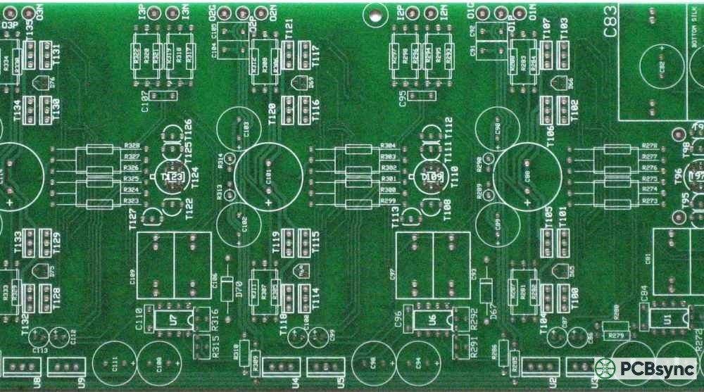
PCB silkscreen (also called the legend layer or nomenclature) is the ink layer printed on your circuit board that contains component designators, polarity markings, logos, and other human-readable information. It’s essentially the user manual printed directly onto your board, and getting it right can mean the difference between smooth production runs and costly assembly errors.
In this guide, I’ll walk you through everything you need to know about PCB silkscreen—from material selection and color choices to design rules and the mistakes I’ve seen derail projects. Whether you’re a hobbyist working on your first board or a seasoned engineer looking to refine your process, you’ll find practical information you can apply immediately.
PCB silkscreen refers to the layer of ink applied to the outer surfaces of a printed circuit board. This layer serves purely informational purposes—it doesn’t affect the electrical characteristics of your board, but it significantly impacts manufacturability, assembly efficiency, and field serviceability.
The term “silkscreen” comes from the traditional printing method where ink was pushed through a silk mesh stencil onto the board surface. While modern PCB manufacturing has largely moved beyond actual silk screens, the name stuck.
Primary Functions of PCB Silkscreen
Your silkscreen layer serves several critical purposes:
Component identification — Reference designators (R1, C5, U3, etc.) help assemblers place components correctly and technicians locate parts during troubleshooting.
Polarity and orientation marking — Indicators for pin 1, cathode stripes, and alignment marks prevent reversed component installation.
Test point labeling — Clearly marked test points speed up debugging and quality control testing.
Branding and documentation — Company logos, part numbers, revision codes, date codes, and certification marks.
Assembly instructions — Jumper settings, configuration notes, and warning symbols.
From a production standpoint, well-designed silkscreen can reduce assembly time by 15-20% and cut down on placement errors significantly. That’s real money when you’re running thousands of boards through an assembly line.
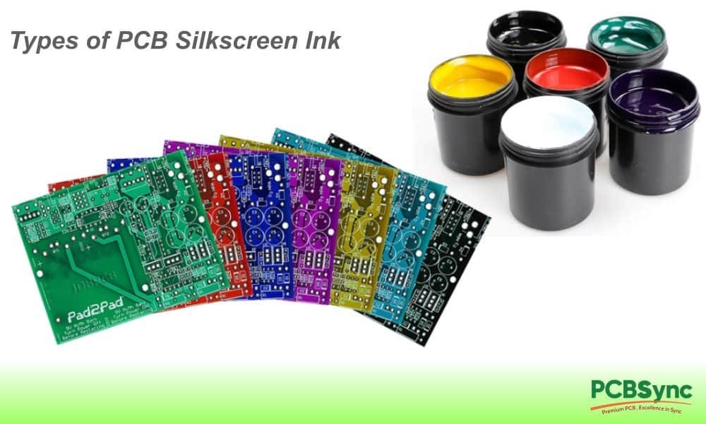
PCB Silkscreen Materials and Ink Types
The ink used for PCB silkscreen isn’t just regular paint. It needs to withstand soldering temperatures, resist chemicals used in manufacturing, and adhere properly to the solder mask surface. Here’s what you need to know about the main types.
Industrial applications requiring chemical resistance
Epoxy-based inks are the industry standard for most applications. They cure through a thermal process and offer excellent adhesion, chemical resistance, and durability. If you’re not sure what to specify, epoxy ink is usually the safe choice.
Acrylic inks cure under UV light, which speeds up production. They’re less expensive but don’t hold up as well under harsh conditions. Fine for consumer products that won’t see extreme temperatures or chemical exposure.
Polyester inks offer superior chemical resistance, making them suitable for industrial environments where boards might be exposed to solvents or cleaning agents.
Silkscreen Ink Properties to Consider
When specifying your PCB silkscreen requirements, consider these properties:
Adhesion strength — How well the ink bonds to the solder mask
Abrasion resistance — Important for boards that will be handled frequently
Chemical resistance — Crucial if the board will be exposed to solvents or cleaning processes
Temperature resistance — Must survive reflow soldering (typically 260°C peak)
Contrast ratio — Readability against the solder mask color
Color selection for PCB silkscreen isn’t just aesthetic—it’s a legibility issue. The goal is maximum contrast against your solder mask color for easy reading under various lighting conditions.
Standard PCB Silkscreen Color Combinations
Solder Mask Color
Recommended Silkscreen
Alternative Options
Avoid
Green
White
Yellow
Green, Black
Blue
White
Yellow
Blue
Black
White
Yellow
Black, Dark colors
Red
White
Yellow, Black
Red
White
Black
Blue, Red
White, Yellow
Yellow
Black
Blue, Red
Yellow, White
Purple
White
Yellow
Purple
Matte Black
White
Yellow (high contrast)
Any dark color
White silkscreen is the industry default and works well with green, blue, red, black, and purple solder masks. It’s the safest choice for most applications.
Black silkscreen is necessary when using white or yellow solder masks. Some designers also use it on green boards for a distinctive look, though contrast is reduced.
Yellow silkscreen provides excellent visibility on darker boards and can be a good alternative to white, particularly for boards that will be inspected under low-light conditions.
Special Color Considerations
Some industries have specific requirements:
Automotive often specifies white on green for standardization
Medical devices may require specific colors for compliance or identification
Military/aerospace typically follows IPC standards with white on green
I generally recommend sticking with white on green unless you have a specific reason to deviate. It’s the most widely used combination, which means suppliers have the most experience with it and problems are less likely.
PCB Silkscreen Printing Methods
How your silkscreen gets applied affects resolution, cost, and durability. Understanding the options helps you make informed decisions and communicate effectively with your fabricator.
Manual Screen Printing (Traditional Method)
The original method uses an actual mesh screen with a stencil of your artwork. Ink is pushed through the mesh onto the board surface.
Pros:
Low setup cost for high volumes
Works well for simple designs
Familiar process at most fab houses
Cons:
Lower resolution (8 mil minimum line width typical)
Registration accuracy limited
Screen wear affects consistency
Liquid Photo Imaging (LPI)
LPI uses a photosensitive ink that’s applied to the entire board, then exposed to UV light through a photomask. Unexposed areas are washed away.
Pros:
Better resolution than manual screening (4-5 mil lines possible)
More consistent results
Good for fine-pitch components
Cons:
Higher cost than manual screening
More complex process
Not available at all fabricators
Direct Legend Printing (DLP) / Inkjet
The newest method uses industrial inkjet technology to print directly onto the board surface. No screens or masks required.
Pros:
Highest resolution (down to 3 mil lines)
No tooling costs
Easy to change designs
Excellent registration
Cost-effective for prototypes and small runs
Cons:
Ink adhesion can be slightly lower
Not all fab houses have the equipment
May have color limitations
For most modern designs, DLP/inkjet is becoming the preferred method. The resolution and flexibility benefits outweigh the minor adhesion trade-off, especially for boards with fine-pitch components where accurate silkscreen placement matters most.
PCB Silkscreen Design Rules and Guidelines
This is where many designers get into trouble. Following proper design rules prevents manufacturing issues and ensures your silkscreen actually serves its purpose.
Critical PCB Silkscreen Design Specifications
Parameter
Minimum Value
Recommended Value
Notes
Text height
0.8 mm (32 mil)
1.0 mm (40 mil)
Smaller text may be illegible
Line width
0.15 mm (6 mil)
0.2 mm (8 mil)
Thinner lines may not print
Text stroke width
0.1 mm (4 mil)
0.15 mm (6 mil)
Varies by font
Clearance from pads
0.1 mm (4 mil)
0.2 mm (8 mil)
Prevents solder contamination
Clearance from vias
0.1 mm (4 mil)
0.15 mm (6 mil)
Unless tented
Clearance from board edge
0.25 mm (10 mil)
0.5 mm (20 mil)
Prevents cutting issues
Font Selection for PCB Silkscreen
Not all fonts work well for silkscreen printing. Here’s what I’ve learned works best:
Recommended fonts:
Vector fonts — Scale cleanly and produce consistent results
Sans-serif fonts — Better legibility at small sizes
Monospace fonts — Useful for aligned data like serial numbers
Fonts to avoid:
Serif fonts (fine details get lost)
Script or decorative fonts
Fonts with very thin strokes
TrueType fonts that don’t convert well to vectors
Most EDA tools have built-in stroke fonts designed specifically for PCB silkscreen. Use them. They’re optimized for this application.
Reference Designator Placement Guidelines
Proper placement of component designators is an art form. Here are the rules I follow:
Place designators adjacent to their component, not on top of it
Maintain consistent orientation — I prefer all text readable from the bottom or right edge
Group related designators — Keep them close but not overlapping
Prioritize readability — If space is tight, prioritize key components
Consider assembly process — Place designators where they’ll be visible after component placement
For dense boards, you may need to make hard choices about what gets labeled. In these cases, prioritize:
Polarized components (ICs, diodes, electrolytics)
Adjustment components (potentiometers, switches)
Test points
Connectors
What to Include on Your PCB Silkscreen
Every board is different, but there are standard elements that should appear on most designs.
Essential PCB Silkscreen Elements
Component reference designators — R1, C5, U3, etc. Follow the schematic naming convention.
Polarity indicators:
Pin 1 dots or notches for ICs
Plus/minus symbols for polarized capacitors
Cathode bars for diodes
Key markings for connectors
Board identification:
Part number
Revision number (REV A, REV B, etc.)
Date code placeholder
Serial number area (if applicable)
Regulatory markings:
CE mark (for European compliance)
FCC ID (for US RF devices)
UL recognition mark
RoHS compliance indicator
Company information:
Company name or logo
Website URL (optional)
Country of origin (required for some markets)
Optional but Useful PCB Silkscreen Elements
Test point labels — TP1, TP2, etc., or signal names like VCC, GND, CLK
Version information — Hardware version, firmware compatibility notes
Assembly notes — “NO CLEAN” indicators, special instructions
Functional labels — INPUT, OUTPUT, POWER, USB, etc. on connectors
Common PCB Silkscreen Mistakes to Avoid
I’ve reviewed thousands of designs over the years. These are the mistakes I see most often.
Mistake #1: Silkscreen Over Pads
This is the cardinal sin of silkscreen design. When silkscreen ink gets on exposed copper pads, it can:
Prevent proper solder wetting
Cause intermittent connections
Lead to solder joint failures
The fix: Set up your DRC (Design Rule Check) to catch silkscreen-to-pad violations. Most EDA tools can do this automatically. Use a minimum clearance of 4 mil, preferably 8 mil.
Mistake #2: Text Too Small to Read
Designers often try to label every component on a dense board, resulting in text so small it’s useless.
The fix: If text must be smaller than 32 mil height, consider:
Using abbreviations
Labeling only critical components
Creating a separate assembly drawing with full designators
Mistake #3: Missing Polarity Indicators
Nothing ruins your day like finding 500 boards with reversed electrolytics because there was no polarity marking.
The fix: Always include polarity indicators for:
All polarized capacitors
Diodes (show cathode)
ICs (pin 1 indicator)
Connectors with key orientation
LEDs
Mistake #4: Silkscreen Over Vias
Unless your vias are tented (covered with solder mask), silkscreen ink can flow into via holes during printing, causing:
Incomplete ink coverage
Messy appearance
Potential contamination issues
The fix: Maintain clearance from exposed vias, or specify tented vias in your fab notes.
Mistake #5: Inconsistent Text Orientation
Boards where some text reads left-to-right, some bottom-to-top, and some upside-down are frustrating to work with during assembly and debugging.
The fix: Establish a convention and stick to it. My preference is all text readable from the bottom or right edge of the board.
Mistake #6: Forgetting the Second Side
Many designers focus on the top silkscreen and forget the bottom layer entirely. If you have bottom-side components, they need proper labeling too.
The fix: Review both silkscreen layers before releasing your design.
Mistake #7: Non-Manufacturing-Ready Artwork
Silkscreen that looks great on screen may not translate to production. Common issues include:
Lines thinner than the fab house can produce
Text converted to fills instead of strokes
Missing clearances at board edges
The fix: Always generate Gerber files and review them with a Gerber viewer before sending to manufacturing.
PCB Silkscreen Design Rules by Manufacturer
Different fabricators have different capabilities. Here’s a comparison of typical silkscreen specifications from major PCB manufacturers:
Manufacturer
Min Line Width
Min Text Height
Min Clearance to Pad
JLCPCB
0.15 mm (6 mil)
0.8 mm (32 mil)
0.1 mm (4 mil)
PCBWay
0.15 mm (6 mil)
0.8 mm (32 mil)
0.15 mm (6 mil)
OSH Park
0.15 mm (6 mil)
1.0 mm (40 mil)
0.15 mm (6 mil)
Eurocircuits
0.12 mm (5 mil)
0.8 mm (32 mil)
0.1 mm (4 mil)
Advanced Circuits
0.15 mm (6 mil)
0.8 mm (32 mil)
0.1 mm (4 mil)
Always check your specific fabricator’s design rules before finalizing your layout. Capabilities vary, and what works at one shop may cause problems at another.
PCB Silkscreen and IPC Standards
If you’re working on professional or certified products, you’ll need to follow IPC standards for silkscreen quality and marking requirements.
Relevant IPC Standards for PCB Silkscreen
IPC-A-610— Acceptability of Electronic Assemblies Defines acceptance criteria for silkscreen quality including:
Legibility requirements
Adhesion standards
Acceptable defects
IPC-2221 — Generic Standard on Printed Board Design Provides guidance on:
Marking content requirements
Text sizing recommendations
Placement guidelines
IPC-6012 — Qualification and Performance Specification for Rigid PCBs Specifies:
Class 1/2/3 requirements for legend quality
Testing methods
Acceptance criteria
For Class 3 (high-reliability) boards, silkscreen requirements are more stringent, with tighter tolerances for legibility, adhesion, and registration accuracy.
Useful PCB Silkscreen Resources and Tools
Here are resources I’ve found valuable over the years:
Design Guidelines and Standards
IPC Designer Certification Program — www.ipc.org — Training and certification for PCB design
PCB Design Guidelines — Most EDA vendors provide application notes on silkscreen best practices
Manufacturer Design Rules — Always download and review your fab house’s specific capabilities
Can PCB silkscreen be removed or modified after manufacturing?
Technically, silkscreen can be removed using abrasive methods or chemical solvents, but I don’t recommend it. Removal attempts typically damage the solder mask underneath or leave visible marks. If you need to correct silkscreen errors, it’s almost always better to respin the board. For prototypes where cost is a major concern, you can sometimes mask over incorrect markings with additional silkscreen ink, but this is a band-aid solution at best.
Does PCB silkscreen affect electrical performance?
No, silkscreen is electrically inert and has no direct effect on your circuit’s performance. The ink is non-conductive and is applied only to the solder mask surface, never on exposed copper. However, silkscreen problems can cause indirect issues—for example, if ink contaminates solder pads during printing, you may experience solder joint failures. This is why maintaining proper clearances is critical.
What’s the minimum feature size for PCB silkscreen?
Most manufacturers can reliably produce 6 mil (0.15 mm) line widths and 32 mil (0.8 mm) text height using standard processes. With DLP/inkjet printing, some fabs can go down to 4 mil lines and 25 mil text, but I recommend designing to 8 mil lines and 40 mil text unless space constraints force otherwise. Remember: just because a fab can produce smaller features doesn’t mean you should specify them.
Should I put silkscreen on both sides of the PCB?
Yes, if you have components on both sides. Bottom-side silkscreen is often neglected, leading to assembly difficulties and increased error rates. Even if your bottom side only has a few passives, having reference designators visible makes hand assembly easier and helps during debugging. The cost difference for adding bottom silkscreen is minimal at most fabricators.
How do I specify silkscreen color in my fabrication notes?
In your fab drawing or order notes, specify both the solder mask color and silkscreen color explicitly. For example: “Solder mask: Green (both sides), Silkscreen: White (both sides).” Don’t assume the fabricator will choose appropriate colors—I’ve seen boards come back with green silkscreen on green solder mask because the color wasn’t specified. When ordering through online PCB services, there’s usually a dropdown menu for these options.
Conclusion
PCB silkscreen might not be the most glamorous aspect of board design, but getting it right pays dividends throughout your product’s lifecycle. From reducing assembly errors to simplifying field repairs, good silkscreen design is a hallmark of professional PCB work.
The key takeaways:
Choose appropriate ink and color combinations for your application and solder mask
Follow design rules — minimum sizes, clearances, and placement guidelines exist for good reasons
Include all necessary information — designators, polarity, identification, and regulatory marks
Avoid common mistakes — especially silkscreen over pads and illegible text
Verify before manufacturing — review Gerbers carefully, including both top and bottom silkscreen layers
Your silkscreen layer is the communication channel between you and everyone who will ever handle your board—assemblers, test technicians, field service engineers, and future designers working on revisions. Make that communication clear, and you’ll avoid countless headaches down the road.
Have questions about a specific silkscreen challenge? Drop them in the comments below—I’m happy to help troubleshoot.
Inquire: Call 0086-755-23203480, or reach out via the form below/your sales contact to discuss our design, manufacturing, and assembly capabilities.
Quote: Email your PCB files to Sales@pcbsync.com (Preferred for large files) or submit online. We will contact you promptly. Please ensure your email is correct.
Notes: For PCB fabrication, we require PCB design file in Gerber RS-274X format (most preferred), *.PCB/DDB (Protel, inform your program version) format or *.BRD (Eagle) format. For PCB assembly, we require PCB design file in above mentioned format, drilling file and BOM. Click to download BOM template To avoid file missing, please include all files into one folder and compress it into .zip or .rar format.


