Inquire: Call 0086-755-23203480, or reach out via the form below/your sales contact to discuss our design, manufacturing, and assembly capabilities.
Quote: Email your PCB files to Sales@pcbsync.com (Preferred for large files) or submit online. We will contact you promptly. Please ensure your email is correct.
Notes: For PCB fabrication, we require PCB design file in Gerber RS-274X format (most preferred), *.PCB/DDB (Protel, inform your program version) format or *.BRD (Eagle) format. For PCB assembly, we require PCB design file in above mentioned format, drilling file and BOM. Click to download BOM template To avoid file missing, please include all files into one folder and compress it into .zip or .rar format.
If you’ve ever wondered how those incredibly precise copper traces get onto a printed circuit board, the answer lies in the PCB photoimaging process. I’ve spent over a decade working in PCB fabrication, and I can tell you that mastering photoimaging is what separates mediocre boards from ones that actually work reliably in the field.
The PCB photoimaging process is essentially a photographic method that transfers circuit patterns onto copper-clad substrates. You expose a light-sensitive material (photoresist) to UV light through a mask or artwork, then develop it to reveal the pattern. What remains protects the copper during etching, giving you your circuit traces.
This guide covers everything from traditional dry film and liquid photoresist methods to modern Laser Direct Imaging (LDI). Whether you’re troubleshooting yield issues in production or setting up a new imaging line, you’ll find practical information here based on real manufacturing experience.
PCB photoimaging is the process of transferring circuit patterns onto a substrate using light-sensitive materials called photoresists. Think of it like photography—you’re essentially “printing” an image onto the board, except instead of paper, you’re working with copper-clad laminate, and instead of ink, you’re creating a protective mask that controls where copper stays and where it gets etched away.
The photoresist undergoes a chemical change when exposed to ultraviolet light (typically 350-400nm wavelength). This change alters its solubility—depending on whether you’re using positive or negative resist, the exposed or unexposed areas become soluble in the developer solution.
Positive vs. Negative Photoresist in PCB Manufacturing
Understanding the difference between positive and negative photoresist is fundamental to PCB photoimaging:
Negative Photoresist: UV light causes cross-linking and hardening. Exposed areas become insoluble and remain after development. This is the most common type in PCB manufacturing due to better adhesion and chemical resistance. Typical exposure dose: 200-400 mJ/cm².
Positive Photoresist: UV light breaks down the chemical structure, making exposed areas soluble. Offers higher resolution (down to 20nm in semiconductor applications) but costs more and requires more careful handling. Typical exposure dose: 50-150 mJ/cm².
For most PCB work, negative resist dominates because it’s more forgiving in production environments and handles the etching chemistry better.
Types of Photoresist Materials for PCB Imaging
Choosing the right photoresist material directly impacts your yield, resolution capability, and production efficiency. Here’s what you need to know about each type.
Dry Film Photoresist: The Industry Workhorse
Dry film photoresist is the go-to choice for most PCB fabricators. It comes as a pre-coated film with a three-layer sandwich structure: a polyester (Mylar) cover sheet on top, the photopolymer resist layer in the middle, and a polyethylene separator on the bottom.
Dry film is available in thicknesses from 0.8 mil (20µm) to 2.0 mil (50µm). For fine-line work below 5 mil trace/space, use thinner films. For hole tenting on multilayer boards, thicker films provide better coverage.
Key advantages of dry film:
Uniform thickness control—critical for consistent etching
Excellent through-hole coverage for tenting
Higher resolution capability (down to 30µm lines/spaces)
Simpler handling and cleaner process
Reduced chemical waste compared to liquid resist
Liquid Photoresist: When Flexibility Matters
Liquid photoresist (also called wet film) is applied by spray coating, roller coating, or curtain coating methods. While it requires more process control than dry film, it offers advantages for certain applications.
Liquid resist works better on uneven surfaces and can be adjusted for thickness during application. Typical dried thickness ranges from 0.5-50 microns depending on the application—thin for high-resolution work, thicker for plating or deep etching.
Application methods for liquid photoresist:
Spray Coating: Fast application with adjustable thickness. Use 30-45 psi air pressure and maintain 3-6 inch spray distance.
Roller Coating: Good for production quantities. Provides consistent coverage but requires careful thickness control.
Curtain Coating: Best for high-volume production. Creates very uniform films but requires significant equipment investment.
Electrodeposition (ED): Uses electrochemical process for ultra-thin, high-resolution coatings on multilayer boards.
Photoresist Comparison Table
Parameter
Dry Film
Liquid Resist
ED Resist
Thickness Range
0.8-2.0 mil (20-50µm)
0.5-50µm (adjustable)
5-15µm
Resolution
30µm lines/spaces
20-50µm lines/spaces
15-25µm lines/spaces
Best Application
General PCB production
Uneven surfaces, custom thickness
HDI, fine-line multilayer
Cost
Medium
Low-Medium
High
Process Complexity
Low
Medium
High
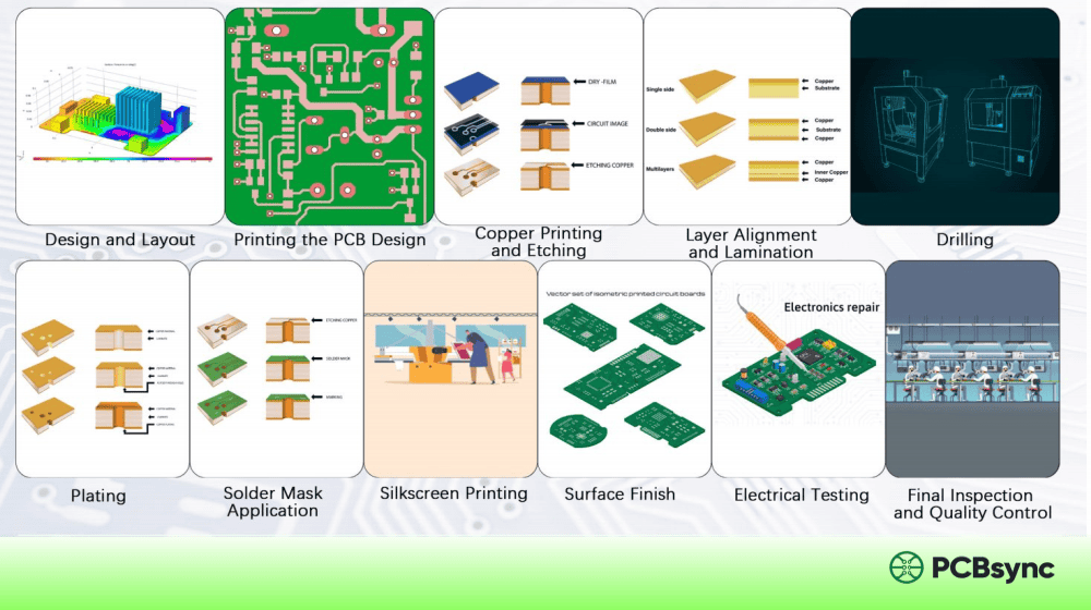
PCB Photoimaging Process: Step-by-Step Workflow
Whether you’re using dry film or liquid resist, the fundamental PCB photoimaging workflow follows the same sequence. Here’s the complete process with the technical parameters that actually matter in production.
Step 1: Surface Preparation
Surface prep is where most imaging failures originate. The copper surface must be absolutely clean and properly textured for resist adhesion.
Mechanical cleaning: Use pumice scrubbing or brushing machines to remove debris and create micro-roughness. Scotch-Brite 96 pads work well for manual cleaning.
Chemical cleaning: Micro-etch with sulfuric acid/hydrogen peroxide to remove oxidation. This creates a chemically active surface for bonding.
Rinse and dry: Use deionized water rinse followed by hot air drying. Any moisture trapped under the resist will cause blisters during etching.
Step 2: Photoresist Application
For dry film lamination:
Cut dry film to match panel size
Remove the bottom polyethylene separator
Hot roll laminate at 105-115°C with controlled pressure
Allow 15+ minutes before removing top cover sheet
Store laminated panels in darkness until exposure
For liquid resist:
Apply resist via spray, roller, or curtain coating
Pre-bake at 70-80°C for 10-20 minutes to remove solvents
Cool to room temperature before exposure
Step 3: UV Exposure
This is where the pattern transfer happens. The photoresist is sensitive to UV-A radiation in the 350-400nm range. Mercury vapor lamps emit at three key wavelengths: i-line (365nm), h-line (405nm), and g-line (435nm).
Critical exposure parameters:
Energy dose: 300-600 mJ/cm² for most dry films. Use a Stouffer 21-step wedge to calibrate—target step held number of 6-8.
Light intensity: 15-30 mW/cm² for standard mask aligners with 350W Hg lamps.
Vacuum contact: Essential for fine-line work. Poor contact causes light scatter and blurred edges.
Collimation: Highly collimated UV sources produce sharper edges. Critical for traces below 5 mil.
Step 4: Development
Development removes the unexposed (for negative resist) or exposed (for positive resist) areas using an alkaline solution, typically 1% sodium carbonate or potassium carbonate.
Spray pressure: Controlled to prevent resist damage
Step 5: Etching and Stripping
After development, the board goes through etching to remove unprotected copper. Common etchants include ferric chloride, cupric chloride, and ammoniacal solutions. The developed resist protects the copper traces you want to keep.
Finally, the remaining resist is stripped using 3-5% sodium hydroxide solution at 45-55°C, revealing the finished copper pattern.
Laser Direct Imaging (LDI): The Modern Alternative
Laser Direct Imaging represents the biggest advancement in PCB photoimaging technology since the industry moved from liquid to dry film resist. LDI eliminates physical phototools entirely, using a computer-controlled laser to write patterns directly onto the photoresist.
How LDI Technology Works
Instead of exposing the entire panel through a photomask, LDI systems use a focused UV laser beam (typically 355-405nm wavelength) to selectively expose the photoresist in a rastering pattern. The system reads digital design files (Gerber data) and translates them directly to the board surface.
Modern LDI systems achieve resolutions down to 10-25 microns for line widths and spacing. The 405nm laser diodes from manufacturers like Nichia and Panasonic are the current industry standard, with optical power potentially reaching 100W per device in future systems.
Medical devices needing ultra-fine features and high reliability
Critical Process Parameters for PCB Photoimaging
Environmental Control Requirements
PCB photoimaging demands controlled environmental conditions. Temperature and humidity fluctuations cause phototool dimensional changes and affect resist performance.
Parameter
Target Range
Critical Impact
Temperature
20-23°C (68-73°F)
Film dimensional stability
Humidity
45-55% RH
Resist adhesion, static control
Clean Room Class
Class 10,000 for ≤5 mil lines
Defect prevention
Lighting
Yellow/amber only
Prevents premature exposure
Exposure Calibration and Monitoring
Regular calibration prevents gradual drift that kills your yield. UV lamp output decreases with age—monitor it with an integrating radiometer like the Dynachem Model 500UV.
Use step tablet testing (Stouffer 21-step or Riston 25-step) to verify exposure. Track the “step held number”—if it drops below specification, adjust exposure time or replace the lamp.
Common PCB Photoimaging Defects and Troubleshooting
After troubleshooting thousands of imaging issues, I’ve found most problems trace back to a handful of root causes. Here’s what to check when things go wrong.
Different industries push PCB photoimaging requirements in different directions. Understanding these applications helps you choose the right process for your specific needs.
Consumer Electronics (Smartphones, Wearables): Demands ultra-fine features with trace widths down to 2/2 mil. LDI is increasingly standard for HDI boards with microvias.
5G Telecommunications: High-frequency signals require precise impedance control. Line width tolerances within ±5 microns are common requirements.
Medical Devices: Miniaturization for implantables demands the highest resolution. Reliability requirements make process control absolutely critical.
Automotive Electronics: Temperature cycling resistance is paramount. Photoimaging must deliver defect-free imaging for safety-critical systems.
Aerospace/Military: Extreme reliability requirements with full process documentation. Often uses more conservative design rules but demands zero defects.
Useful Resources and Standards
For engineers looking to deepen their knowledge of PCB photoimaging, these resources provide essential reference material.
Industry Standards:
IPC-9121: Troubleshooting for Printed Board Fabrication Processes—comprehensive defect analysis and solutions
IPC-6012: Qualification and Performance Specification for Rigid Printed Boards
IPC-A-600: Acceptability of Printed Boards—visual quality standards
Photoresist Manufacturers (Technical Data and Process Guides):
What is the minimum line width achievable with PCB photoimaging?
With traditional photolithography using dry film, practical production limits are around 3/3 mil (75µm) lines and spaces. LDI systems can achieve 2/2 mil (50µm) or finer in production environments. For leading-edge HDI work, some processes push below 25µm, though this requires specialized equipment and extremely tight process control.
How do I determine the correct exposure dose for my photoresist?
Use a step transmission wedge (Stouffer 21-step or similar) to calibrate exposure. The correct dose shows proper crosslinking with the step held number matching the resist manufacturer’s specification—typically 6-8 steps for most dry films. If you have an integrating UV radiometer, target 300-600 mJ/cm² for standard dry films, adjusting based on your specific material and equipment.
When should I switch from traditional photoimaging to LDI?
Consider LDI when: (1) Your designs regularly require trace widths below 5/5 mil, (2) You’re doing significant prototype work with frequent design iterations, (3) Registration between layers is becoming a yield limiter, or (4) Phototool management costs are significant. The higher equipment cost of LDI typically pays back through improved yield and faster setup times for HDI and prototype work.
What causes the most common photoimaging failures?
In my experience, about 70% of imaging failures trace back to surface preparation issues—contamination, insufficient micro-etch, or moisture. Another 20% come from exposure problems (wrong dose, poor contact, light scatter). The remaining 10% split between development issues and material defects. Always start troubleshooting with surface prep before looking elsewhere.
Can I use the same photoresist for inner layers and outer layers?
Yes, the same dry film can generally be used for both, but the process parameters differ. Outer layers often require thicker resist for plating resistance and may use different exposure doses. Inner layer imaging is typically more straightforward since you’re just creating etch resist. Some fabricators use lower-cost films for inner layers where resolution requirements are less demanding.
Conclusion
The PCB photoimaging process remains the foundation of circuit board manufacturing, whether you’re using traditional dry film, liquid resist, or cutting-edge LDI technology. Success comes down to understanding the chemistry, controlling your parameters, and maintaining rigorous process discipline.
As electronic devices continue shrinking and HDI boards become more common, imaging capability increasingly determines what’s possible in PCB fabrication. Investing in the right technology and process control for your application isn’t just about quality—it’s about staying competitive in an industry that never stops pushing toward finer features and higher density.
Whether you’re optimizing an existing line or evaluating LDI for fine-line production, the fundamentals covered in this guide will help you make informed decisions and troubleshoot problems when they arise. Good imaging is the starting point for good boards.
Future Trends in PCB Photoimaging Technology
The PCB photoimaging landscape continues to evolve rapidly as electronic devices demand ever-smaller features and higher density interconnects. Several key trends are shaping where this technology is headed over the next five to ten years.
Advanced LDI Systems and Higher Resolution
Current LDI systems already achieve resolutions around 10-25 microns, but the push toward sub-10 micron line widths is driving new developments. Multi-wavelength LDI systems that utilize different laser wavelengths concurrently are improving versatility and precision. Real-time adaptive imaging technology dynamically adjusts laser parameters during exposure to compensate for substrate variations, ensuring more consistent results across entire panels.
The mainstream 405nm laser diodes are expected to see optical power improvements, potentially reaching 100W per single device. This increased power translates directly to faster throughput without sacrificing image quality—a critical factor for production economics.
New Photoresist Chemistries
Photoresist manufacturers are developing new chemistries specifically optimized for LDI applications. These LDI-specific resists feature faster reaction kinetics to match the high scan speeds of laser systems, improved sensitivity at targeted wavelengths, and better contrast characteristics that enable sharper edge definition.
Environmentally friendly photoresist formulations are also gaining traction. These newer materials reduce or eliminate hazardous chemicals in both the resist itself and the developer solutions required for processing. As environmental regulations tighten globally, these green chemistry approaches will become increasingly important for PCB fabricators.
Integration with Industry 4.0 Manufacturing
Modern PCB photoimaging systems are becoming connected nodes in smart factory environments. Real-time process monitoring captures exposure parameters, development conditions, and yield data for every panel. Machine learning algorithms analyze this data to predict potential defects before they occur and optimize process parameters continuously.
Automated inspection systems integrated directly with imaging lines provide immediate feedback on imaging quality. When combined with closed-loop control systems, this enables automatic adjustment of exposure doses, development times, and other parameters to maintain optimal quality without operator intervention.
Process Optimization Tips from the Production Floor
Beyond the fundamental process parameters, here are some practical tips that can make a real difference in your imaging quality and yield.
Material Handling Best Practices
Dry film photoresist is sensitive to temperature, humidity, and mechanical stress. Store dry film rolls at 15-25°C and 45-65% relative humidity. Allow refrigerated material to equilibrate to room temperature before opening to prevent condensation. Handle rolls by the core only—fingerprints on the resist surface will cause imaging defects.
For liquid photoresist, shelf life is typically 6-12 months for unopened containers stored at room temperature in darkness. Once opened or diluted, use within a few days. Discard any resist that becomes stringy, gels, or forms visible sludge—using degraded material will create inconsistent results and defects.
Phototool Management for Traditional Imaging
If you’re using traditional photolithography with physical phototools, their condition directly impacts your imaging quality. Inspect phototools regularly for scratches, pinholes, contamination, and dimensional stability. Even minor defects on the phototool will transfer to every board you expose.
Store phototools flat in protective sleeves at controlled temperature and humidity. Track usage and replace films that show signs of wear or dimensional drift. For high-volume production, consider investing in glass phototools—they’re more expensive but offer superior dimensional stability and longer life.
Development Process Control
Many fabricators focus heavily on exposure optimization while neglecting development. But under-development leaves resist residue that causes poor etching, while over-development attacks the edges of your intended pattern and degrades resolution.
Monitor your developer solution concentration continuously—it degrades as dissolved resist accumulates. Use conductivity or titration methods to track concentration and add makeup solution or replace the bath before it drifts out of specification. Maintaining developer at the correct concentration is just as important as hitting your exposure dose.
Equipment Maintenance Schedule
Preventive maintenance keeps imaging equipment performing consistently. For exposure systems, track UV lamp hours and monitor intensity—most lamps lose 10-15% output over their rated life. Clean exposure glass and vacuum systems weekly to prevent contamination from affecting contact quality.
For lamination equipment, verify roller pressure and temperature monthly. Worn or contaminated rollers cause uneven resist application and adhesion problems. Developer systems require regular cleaning of spray nozzles and verification of solution flow rates. Clogged nozzles create non-uniform development that shows up as line width variation.
This summary table provides at-a-glance reference for the key parameters discussed throughout this guide.
Process Step
Key Parameter
Typical Value
Lamination
Temperature
105-115°C
Lamination
Hold time before exposure
≥15 minutes
UV Exposure
Wavelength
350-400nm (UV-A)
UV Exposure
Energy dose (dry film)
300-600 mJ/cm²
UV Exposure
Step held number target
6-8 steps
Development
Na₂CO₃ concentration
0.8-1.2%
Development
Temperature
28-32°C
Stripping
NaOH concentration
3-5%
Stripping
Temperature
45-55°C
Environment
Room temperature
20-23°C
Environment
Relative humidity
45-55% RH
LDI
Laser wavelength
355-405nm
LDI
Resolution capability
10-25µm
Remember that these values serve as starting points—your specific equipment, materials, and quality requirements may necessitate adjustments. Always validate parameters with your actual production conditions and consult material data sheets for specific photoresist products.
Inquire: Call 0086-755-23203480, or reach out via the form below/your sales contact to discuss our design, manufacturing, and assembly capabilities.
Quote: Email your PCB files to Sales@pcbsync.com (Preferred for large files) or submit online. We will contact you promptly. Please ensure your email is correct.
Notes: For PCB fabrication, we require PCB design file in Gerber RS-274X format (most preferred), *.PCB/DDB (Protel, inform your program version) format or *.BRD (Eagle) format. For PCB assembly, we require PCB design file in above mentioned format, drilling file and BOM. Click to download BOM template To avoid file missing, please include all files into one folder and compress it into .zip or .rar format.


