Inquire: Call 0086-755-23203480, or reach out via the form below/your sales contact to discuss our design, manufacturing, and assembly capabilities.
Quote: Email your PCB files to Sales@pcbsync.com (Preferred for large files) or submit online. We will contact you promptly. Please ensure your email is correct.
Notes: For PCB fabrication, we require PCB design file in Gerber RS-274X format (most preferred), *.PCB/DDB (Protel, inform your program version) format or *.BRD (Eagle) format. For PCB assembly, we require PCB design file in above mentioned format, drilling file and BOM. Click to download BOM template To avoid file missing, please include all files into one folder and compress it into .zip or .rar format.
If you’ve ever wondered what’s really happening inside your printed circuit boards, you’re not alone. After 15 years of working with PCB fabrication and quality control, I can tell you that surface inspections only tell half the story. The real secrets—the plating thickness, the via integrity, the layer alignment—they’re all hidden beneath the surface. That’s where PCB microsection analysis comes in.
In this guide, I’ll walk you through everything you need to know about PCB microsection testing: the process, the equipment, the defects you’ll find, and why this destructive test might just save your next project from costly field failures.
PCB microsection analysis (also called cross-section analysis or metallographic preparation) is a destructive testing method that reveals the internal structure of a printed circuit board. By cutting a small sample from the board, mounting it in epoxy resin, and polishing it to a mirror finish, we can examine what’s really going on inside—layer by layer, micron by micron.
Think of it like a biopsy for your circuit board. Just as a doctor examines tissue samples to diagnose problems, we examine PCB cross-sections to identify PCB manufacturing defects, verify process quality, and understand why boards fail.
Why PCB Microsection Testing Matters
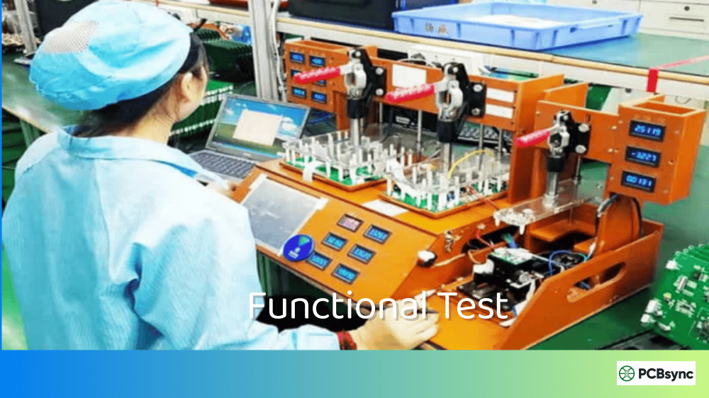
Here’s the reality: non-destructive testing methods like X-ray inspection and AOI (Automated Optical Inspection) are fantastic for production screening, but they have limits. X-rays can show you shadows and outlines, but they can’t measure copper plating thickness with precision or reveal microscopic cracks in via barrels.
PCB microsection analysis provides:
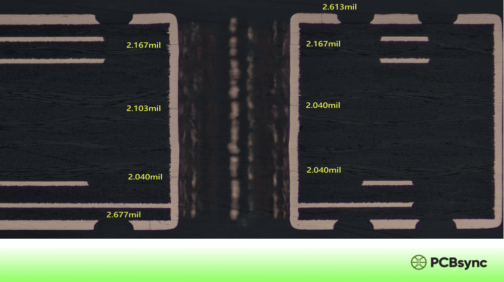
Precise measurements of copper thickness (typically 25-35 µm for standard boards)
Visual confirmation of layer-to-layer alignment (tolerances as tight as ±50 µm)
Defect identification that’s impossible to see any other way
Process validation for drilling, plating, and lamination
Failure analysis when boards don’t perform as expected
For Class 3 applications—medical devices, aerospace systems, military equipment—microsection testing isn’t optional. It’s mandatory.
When Should You Perform PCB Microsection Analysis?
Not every board needs cross-sectioning. Here’s when it makes sense:
During Manufacturing Process Development
When you’re dialing in a new process—whether it’s laser drilling microvias or implementing a new plating chemistry—microsection analysis helps you validate that your parameters are producing the results you expect.
For First Article Inspection
Before releasing a new design to volume production, cross-sectioning a few test coupons confirms that the fabricator can meet your specifications. This is especially critical for high-layer-count boards or HDI designs with blind and buried vias.
During Production Quality Control
Most manufacturers run microsection analysis on a sampling basis—typically pulling test coupons from production panels at defined intervals to monitor process stability.
For Failure Analysis
When a board fails in the field or during testing, microsection analysis often reveals the root cause. Was it a plating void? Barrel cracking from thermal stress? Delamination between layers? The cross-section tells the story.
Let me walk you through how we actually perform cross-section analysis in the lab. The process is straightforward but demands precision at every step.
Step 1: Sample Selection and Cutting
First, we identify the area of interest. For routine quality control, this is usually a test coupon—a small section of the panel designed specifically for destructive testing. For failure analysis, we target the suspected defect location.
Using a precision diamond saw with coolant (to prevent thermal damage), we cut a sample approximately 10-15 mm in width. The cut must be clean and perpendicular to avoid introducing stress or distortion.
Step 2: Mounting and Encapsulation
The sample is placed in a mounting cup and encapsulated in clear epoxy resin. This serves two purposes: it protects the sample during grinding and provides a stable surface to work with. The epoxy must fully infiltrate any holes or voids—vacuum impregnation helps ensure complete fill.
After pouring, the epoxy cures (typically overnight or with heat acceleration) to form a solid “puck” with the PCB sample embedded inside.
Step 3: Grinding and Polishing
This is where skill and patience matter most. We progressively remove material to expose the plane of interest—usually the center of a plated through-hole or via.
Stage
Grit/Abrasive
Purpose
Coarse grinding
240 grit SiC
Rapid material removal to approach target
Medium grinding
400-600 grit SiC
Refine surface, remove deep scratches
Fine grinding
800-1200 grit SiC
Prepare for polishing
Initial polish
6 µm diamond
Remove grinding scratches
Intermediate polish
1 µm diamond/alumina
Achieve near-mirror finish
Final polish
0.3-0.05 µm alumina
Mirror finish for microscopy
Between each step, we clean the sample thoroughly to prevent cross-contamination. The goal is to reach the center of the target feature—no more than 10% beyond the plated through-hole’s center, per IPC guidelines.
Step 4: Etching (Optional)
For certain analyses, we apply a light chemical etch to enhance contrast between different metals and reveal grain structures. A common etchant for copper is a dilute solution of ammonia and hydrogen peroxide (5-10 mL ammonia + 45 mL DI water + 2-3 drops H₂O₂).
The etch is applied briefly—just 2-3 seconds—then immediately rinsed and dried. Over-etching causes oxidation and obscures details.
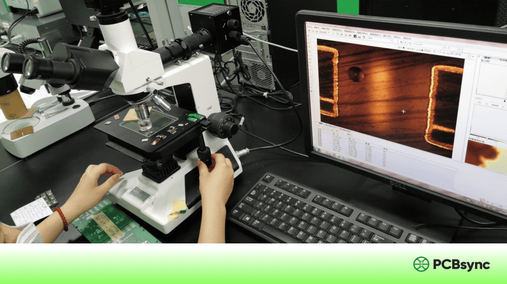
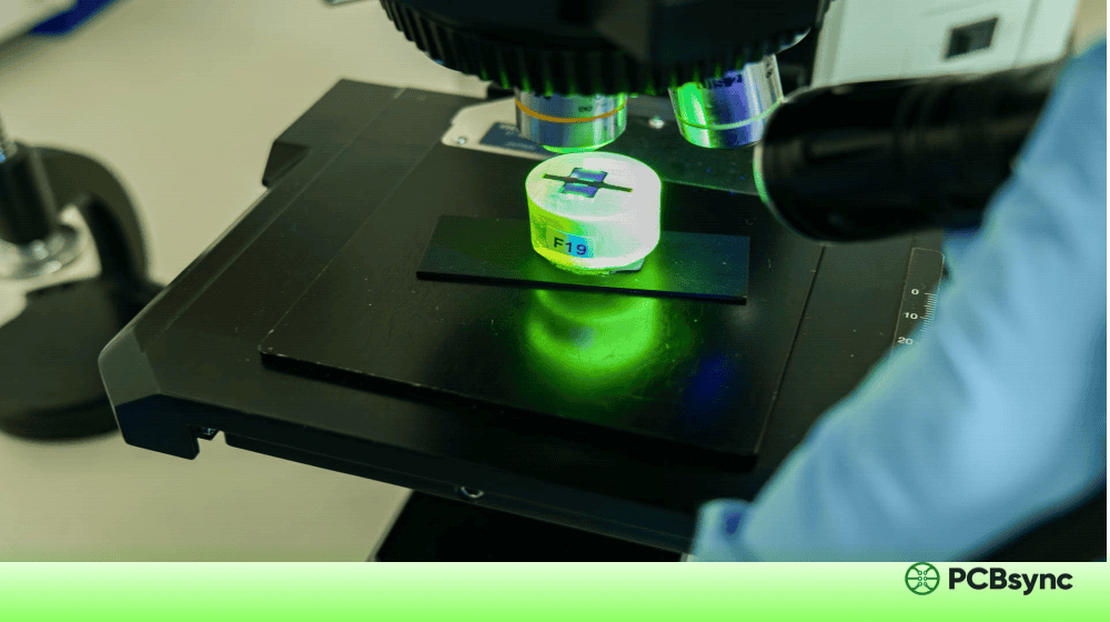
Step 5: Microscopic Examination
Finally, we examine the polished cross-section under a metallurgical microscope at magnifications from 50x to 1000x. Digital imaging systems capture photos for documentation and measurement.
For advanced analysis, we might use:
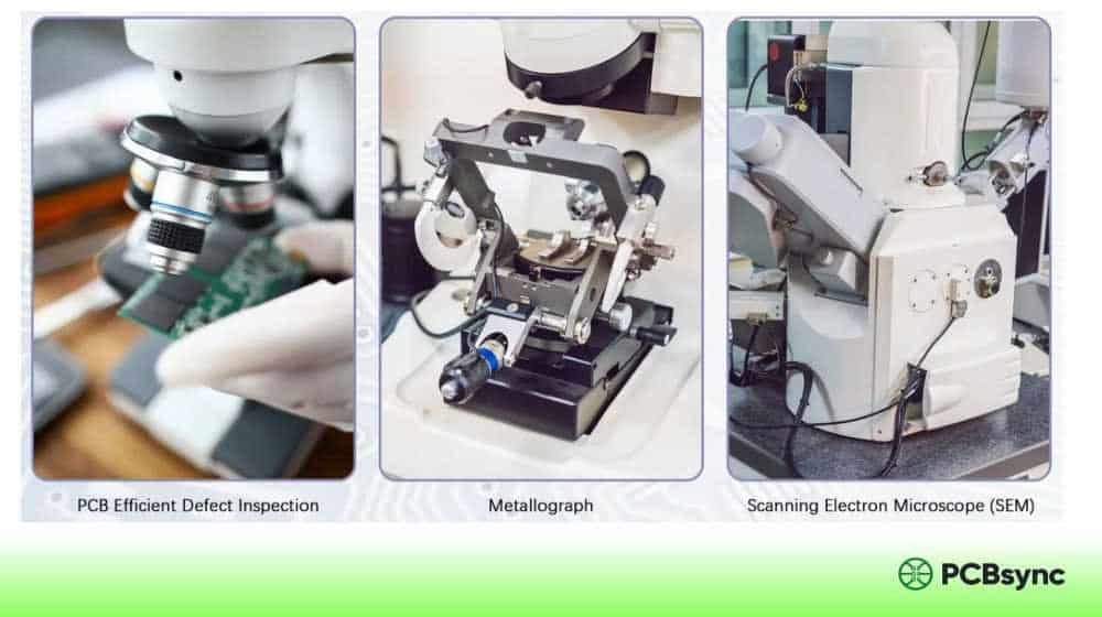
SEM (Scanning Electron Microscope): Higher magnification and depth of field
Polarized light: Stress patterns and grain structure
Essential Equipment for PCB Microsection Analysis
Setting up a microsection lab requires specialized equipment. Here’s what you’ll need:
Cutting Equipment
Equipment
Function
Key Features
Precision sectioning saw
Sample extraction
Diamond blade, adjustable speed, coolant system
Abrasive cutoff wheel
Rough cuts
Fast but less precise
Sample Preparation Equipment
Equipment
Function
Key Features
Mounting press
Epoxy encapsulation
Temperature control, vacuum capability
Grinding/polishing machine
Surface preparation
Variable speed, multiple platens
Ultrasonic cleaner
Inter-step cleaning
Removes debris and contamination
Inspection Equipment
Equipment
Function
Magnification Range
Metallurgical microscope
Primary inspection
50x – 1000x
Stereo microscope
Sample overview
5x – 50x
Digital camera system
Documentation
High-resolution imaging
SEM
Advanced analysis
10x – 2000x+
For high-volume operations, automated grinding and polishing systems improve consistency and throughput. Some labs process 20+ samples per day using programmed polishing sequences.
Common Defects Revealed by PCB Microsection Analysis
Here’s where the real value of cross-sectioning becomes clear. These are the defects we routinely identify:
Plating Defects
Defect
Description
Cause
Impact
Plating voids
Gaps in copper plating on via walls
Poor surface prep, air bubbles, contamination
Electrical discontinuity, reliability failures
Thin plating
Copper thickness below spec (<25 µm)
Insufficient plating time, bath chemistry issues
Increased resistance, thermal failures
Nodules
Rough protrusions in plating
Contamination in plating bath
Signal integrity issues in high-speed designs
Barrel cracking
Cracks in via barrel wall
Thermal stress, Z-axis expansion
Intermittent connections, field failures
Laminate Defects
Defect
Description
Cause
Impact
Delamination
Layer separation
Poor bonding, moisture absorption, thermal stress
Mechanical weakness, moisture ingress
Voids
Air pockets in dielectric
Improper lamination, contamination
Reduced dielectric strength
Measling
White spots in laminate
Resin-fiber separation
Cosmetic (usually); may indicate process issues
Crazing
Fine cracks in resin
Mechanical or thermal stress
Potential moisture paths
Registration and Alignment Issues
Defect
Description
Cause
Impact
Layer misregistration
Inner layers not aligned to holes
Scaling errors, material movement
Reduced annular ring, connectivity issues
Drill wander
Holes not perpendicular
Worn bits, improper parameters
Registration problems on inner layers
Resin smear
Epoxy residue on inner layer copper
Drilling heat, inadequate desmear
Poor electrical connection
Solder Joint Defects
Defect
Description
Cause
Impact
Voids in solder
Gas pockets within joint
Outgassing, flux residue
Reduced thermal/electrical performance
Insufficient wetting
Poor solder coverage
Contamination, poor solderability
Weak mechanical connection
Kirkendall voids
Voids at intermetallic interface
Diffusion during aging
Long-term reliability issues
Cold joints
Grainy, dull solder structure
Insufficient heat, movement during solidification
Intermittent failures
IPC Standards for PCB Microsection Analysis
Understanding the relevant standards is crucial for interpreting your results and communicating with suppliers.
Key IPC Standards
Standard
Purpose
IPC-A-600
Acceptability of Printed Boards – Visual illustrations of acceptable/rejectable conditions
IPC-6012
Qualification and Performance Specification for Rigid PCBs
IPC-TM-650 2.1.1
Test method for microsection preparation
IPC-A-610
Acceptability of Electronic Assemblies (includes solder joint criteria)
IPC Classification System
IPC defines three classes based on end-use requirements:
Medical, military, aerospace – zero tolerance for defects
For Class 3 boards, IPC-6012 specifies minimum copper plating thickness of 25 µm in plated through-holes, with no voids exceeding specific limits. The microsection is the definitive method for verifying compliance.
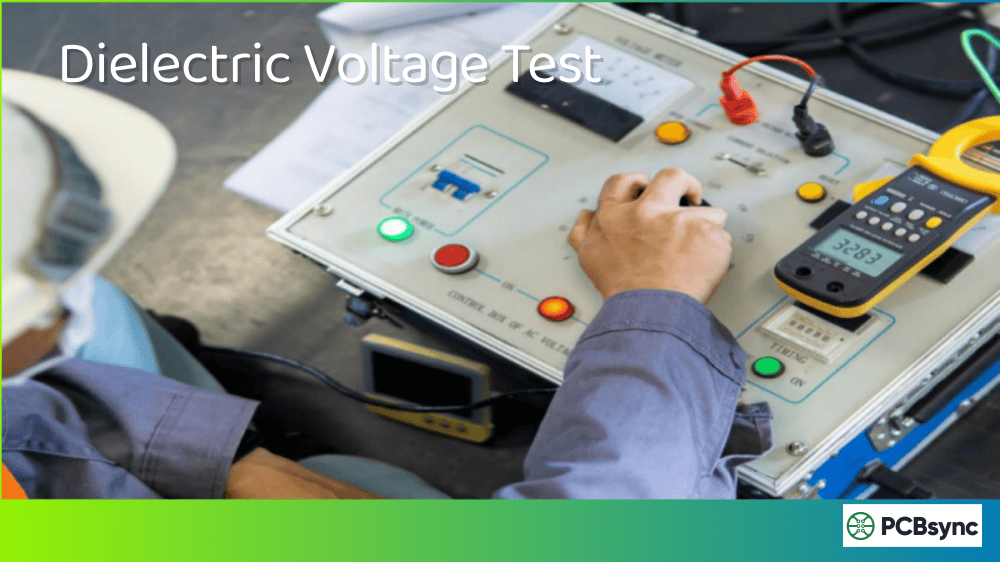
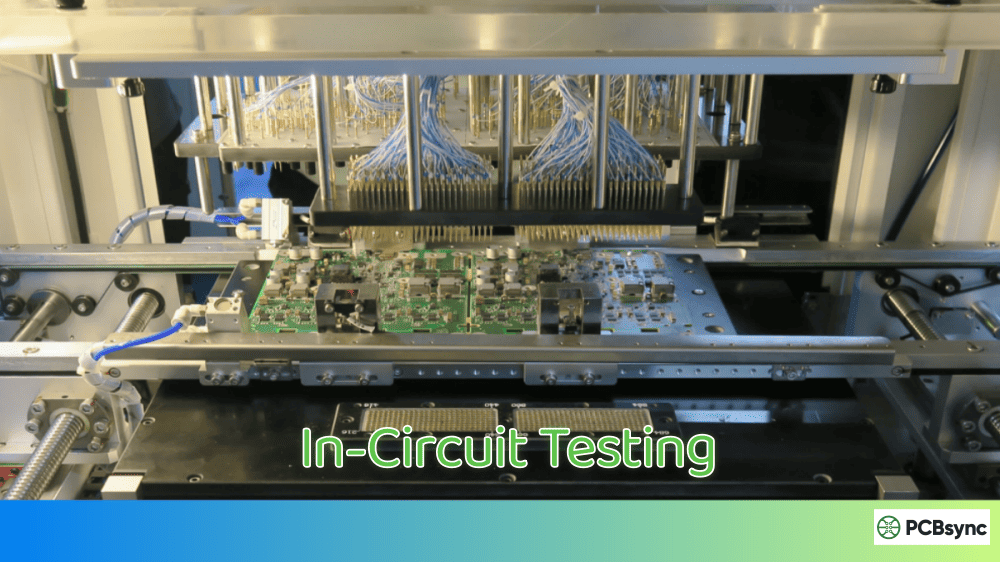
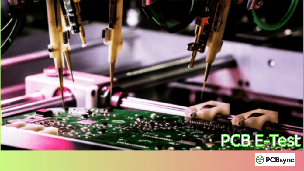
How does microsection analysis compare to other testing approaches?
Method
Type
What It Reveals
Limitations
PCB Microsection
Destructive
Complete internal structure, precise measurements
Destroys sample, time-consuming
X-ray Inspection
Non-destructive
Internal features, BGA voids, hidden shorts
Limited resolution, 2D projection issues
AOI
Non-destructive
Surface defects, component placement
Surface only, can’t see internal features
Electrical Test
Non-destructive
Continuity, isolation, opens/shorts
Doesn’t show physical structure
CT Scanning
Non-destructive
3D internal structure
Expensive, lower resolution than microsection
The bottom line: microsection analysis remains the gold standard for internal quality verification. When you need definitive answers about what’s inside your PCB, nothing else comes close.
Best Practices for PCB Microsection Analysis
After years of doing this work, here are the practices that separate good microsection analysis from great:
Sample Preparation
Use test coupons whenever possible—don’t destroy good boards unnecessarily
Document sample location before cutting for traceability
Control temperature during cutting to prevent thermal damage
Allow adequate epoxy cure time before grinding
Grinding and Polishing
Progress through grits systematically—don’t skip steps
Clean thoroughly between stages to prevent cross-contamination
Check progress frequently under the microscope
Stop at the correct plane—overshooting wastes valuable data
Analysis and Reporting
Calibrate measurement software regularly
Take multiple measurements and report averages
Photograph all observations at appropriate magnifications
Reference applicable IPC criteria in reports
Useful Resources for PCB Microsection Analysis
Here are resources I recommend for anyone working in this field:
Industry Standards (Available from IPC)
IPC-A-600M (Latest revision) – Acceptability of Printed Boards
IPC-6012E – Qualification and Performance Specification for Rigid PCBs
IPC-TM-650 – Test Methods Manual (includes microsectioning procedures)
ASM Handbook Volume 9: Metallography and Microstructures
IPC Designer’s Council webinars on cross-section analysis
Frequently Asked Questions About PCB Microsection
What is the typical cost of PCB microsection analysis?
Basic microsection analysis typically costs $100-500 per sample, depending on complexity and reporting requirements. Advanced analysis with SEM/EDS can run $500-1,000 or more. High-volume testing from the same batch often qualifies for volume discounts. The cost is negligible compared to the expense of field failures or product recalls.
How long does PCB microsection analysis take?
Standard turnaround is 2-5 business days. Some labs offer rush service (1-2 days) at premium pricing. The actual prep work takes 4-8 hours per sample, but most of that is epoxy curing time and sequential polishing steps.
Can microsection analysis be automated?
Partially. Automated grinding and polishing systems improve consistency and throughput, and some labs are exploring AI-assisted image analysis for defect detection. However, sample cutting, mounting, and final microscopic evaluation still require skilled human judgment.
What sample size is needed for PCB microsection?
A typical sample is 10-15 mm square, large enough to include the features of interest (via, PTH, trace) plus margin for mounting and grinding. Test coupons are usually designed to approximately 25 mm (1 inch) square.
How do microsection results compare to X-ray inspection?
They’re complementary, not competitive. X-ray provides non-destructive screening of 100% of production, while microsection provides definitive verification on samples. X-ray might show a shadow suggesting a void; microsection confirms it, measures it, and identifies its cause.
Conclusion
PCB microsection analysis isn’t glamorous work, but it’s essential. Every time I cut into a board and see the layers revealed under the microscope, I’m reminded why this technique has remained the industry standard for decades. No other method gives you the same combination of precision, detail, and definitive answers about internal board quality.
Whether you’re validating a new fabrication process, investigating a field failure, or ensuring compliance with Class 3 requirements, microsection analysis provides the evidence you need. The investment in proper equipment, trained personnel, and systematic procedures pays dividends in product reliability and customer confidence.
If you’re not already incorporating cross-section analysis into your quality program, it’s time to start. Your boards—and your customers—will thank you.
Inquire: Call 0086-755-23203480, or reach out via the form below/your sales contact to discuss our design, manufacturing, and assembly capabilities.
Quote: Email your PCB files to Sales@pcbsync.com (Preferred for large files) or submit online. We will contact you promptly. Please ensure your email is correct.
Notes: For PCB fabrication, we require PCB design file in Gerber RS-274X format (most preferred), *.PCB/DDB (Protel, inform your program version) format or *.BRD (Eagle) format. For PCB assembly, we require PCB design file in above mentioned format, drilling file and BOM. Click to download BOM template To avoid file missing, please include all files into one folder and compress it into .zip or .rar format.


