Inquire: Call 0086-755-23203480, or reach out via the form below/your sales contact to discuss our design, manufacturing, and assembly capabilities.
Quote: Email your PCB files to Sales@pcbsync.com (Preferred for large files) or submit online. We will contact you promptly. Please ensure your email is correct.
Notes: For PCB fabrication, we require PCB design file in Gerber RS-274X format (most preferred), *.PCB/DDB (Protel, inform your program version) format or *.BRD (Eagle) format. For PCB assembly, we require PCB design file in above mentioned format, drilling file and BOM. Click to download BOM template To avoid file missing, please include all files into one folder and compress it into .zip or .rar format.
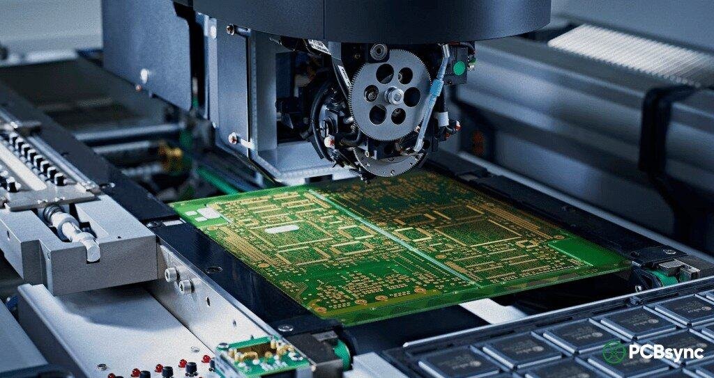
After spending over a decade in the electronics industry, I’ve walked through countless PCB fabrication facilities and watched boards transform from raw copper-clad laminates into the intricate circuits powering everything from smartphones to satellites. The PCB manufacturing process remains one of the most fascinating and complex procedures in modern electronics production. Whether you’re a design engineer looking to optimize your layouts for manufacturability or someone new to the industry trying to understand how printed circuit boards come to life, this guide breaks down every critical step.
Understanding the complete PCB manufacturing process isn’t just academic curiosity—it’s practical knowledge that directly impacts your designs. When you know what happens at each stage, you can make smarter decisions during the design phase, avoid costly mistakes, and communicate more effectively with your fabrication partners.
What is PCB Manufacturing?
PCB manufacturing is the multi-stage industrial process that transforms design files into physical printed circuit boards. It involves converting electronic design data—typically Gerber or ODB++ files—into a fabricated board through a precise sequence of chemical, mechanical, and photolithographic processes.
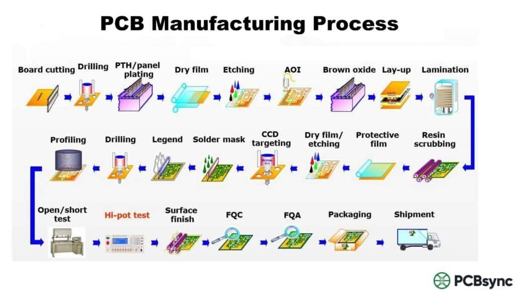
The complexity of this process varies significantly based on board type. A simple single-layer board might require around 10 steps, while a complex 20-layer HDI (High-Density Interconnect) board with blind and buried vias could involve 30 or more individual manufacturing stages. The key principle remains constant: every step must be executed with precision, because errors compound and can render entire production batches unusable.
Let’s walk through each stage of the PCB manufacturing process in detail. I’ll explain not just what happens at each step, but why it matters and what can go wrong if it’s not done correctly.
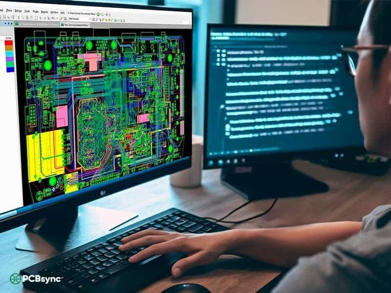
Step 1: Design and Schematic Capture
Every PCB starts as an idea that gets translated into a schematic diagram—the electrical blueprint showing component connections. Engineers use Electronic Design Automation (EDA) software like Altium Designer, KiCad, Eagle, or OrCAD to create both the schematic and the subsequent PCB layout.
The design phase includes component placement optimization, trace routing (manual, semi-automatic, or auto-interactive), and extensive Design Rule Checks (DRC). These automated checks verify that your design meets manufacturing tolerances for trace width, spacing, hole sizes, and clearances.
Pro Tip: Always communicate with your fabricator early. Many issues I’ve seen could have been avoided if designers had run their plans past the manufacturing team before finalizing layouts. Most PCB manufacturers offer free Design for Manufacturing (DFM) reviews—use them.
Step 2: Design File Output and DFM Review
Once the design is complete, it’s exported in a format manufacturers can process. Extended Gerber (RS-274X) remains the most common format, though ODB++ and IPC-2581 are gaining traction for their ability to carry more comprehensive design intent information.
The manufacturing data package typically includes Gerber files for each copper layer, solder mask layers, silkscreen layers, drill files (Excellon format), a netlist for electrical testing, and fabrication notes specifying materials, finishes, and tolerances.
Before production begins, manufacturers perform a thorough DFM check. This catches issues like traces too close to board edges, holes too small for reliable plating, or copper features that might cause acid traps during etching. Getting this right saves enormous headaches down the line.
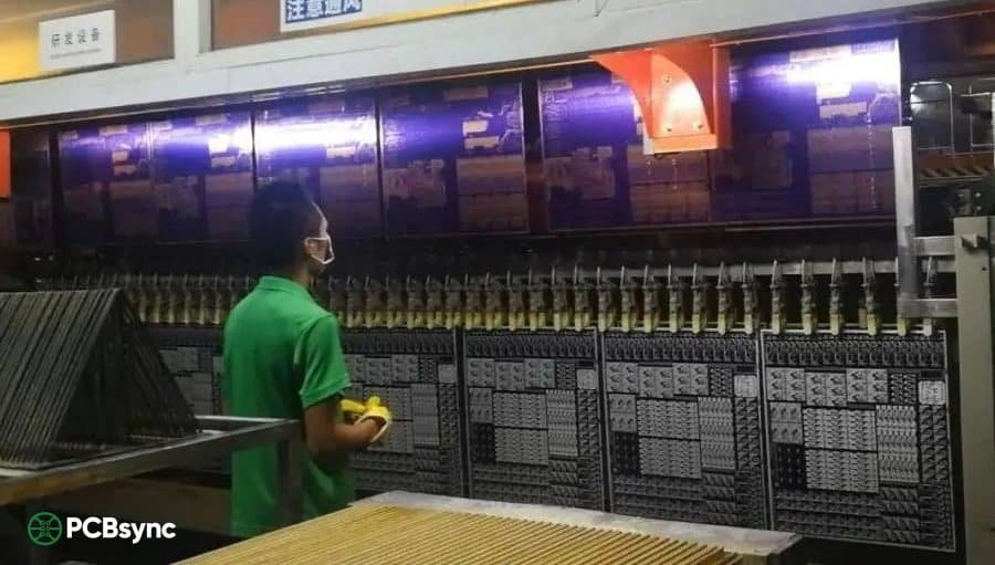
Step 3: Film Generation and Imaging
The manufacturer converts your design data into physical photo films or prepares it for Laser Direct Imaging (LDI). Traditional photo films are produced using precision laser plotters that create transparent sheets with your circuit pattern in opaque ink.
For inner layers, black ink represents conductive copper areas, while clear areas will be etched away. This convention reverses for outer layers. Registration holes are punched through all films to ensure perfect alignment between layers—a critical requirement for multilayer boards where even slight misalignment causes connection failures.
Modern facilities increasingly use LDI, which projects the pattern directly onto photoresist-coated panels using computer-controlled lasers. This eliminates film-related issues and allows rapid design changes without reprinting physical films.
Step 4: Inner Layer Preparation and Printing
The actual board fabrication begins here. For multilayer boards, we start with the inner layers. The base material—typically FR-4 (glass-reinforced epoxy laminate)—comes pre-clad with copper foil on both sides.
The copper-clad laminate is first cleaned in a controlled environment. Any contamination at this stage can cause defects. The panel is then coated with a photosensitive film called photoresist. This light-sensitive material hardens when exposed to UV light and remains soft in unexposed areas.
The film or LDI system exposes the photoresist, transferring the circuit pattern. Where UV light hits (through the clear areas of the film), the resist hardens and will protect the underlying copper during etching.
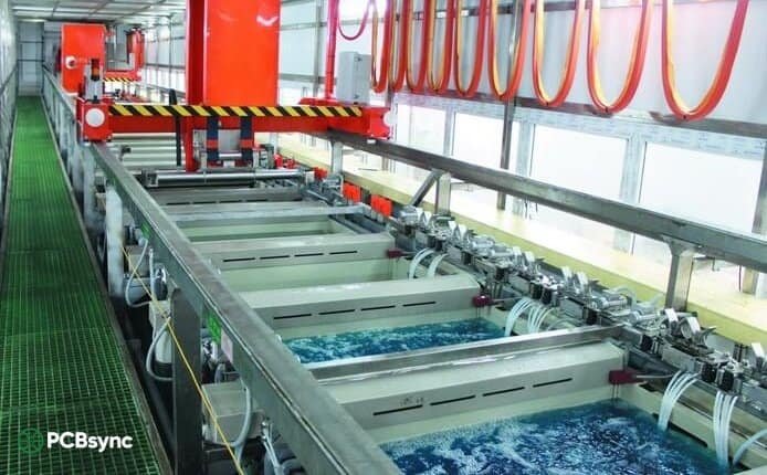
Step 5: Etching the Inner Layers
After exposure and development (which removes unhardened photoresist), the panels enter the etching line. This is where excess copper gets removed, leaving only the desired circuit traces.
The process happens in a conveyorized develop-etch-strip (DES) line. Chemical etchants—typically acidic cupric chloride or alkaline ammonia-based solutions—dissolve exposed copper while the hardened resist protects the circuit pattern beneath.
Etching chemistry must be carefully controlled. Temperature, concentration, and spray pressure all affect etch uniformity. Under-etching leaves unwanted copper; over-etching undercuts traces and reduces conductor width. Either can render a board unusable.
Step 6: Automated Optical Inspection (AOI)
Before proceeding, each inner layer undergoes Automated Optical Inspection. High-resolution cameras scan the etched panels and compare them against the original Gerber data. This catches opens, shorts, scratches, and other defects before they’re buried inside a laminated stack.
This step is critical because once layers are laminated together, inner layer defects cannot be repaired. Any defective panels are scrapped at this stage rather than wasting additional processing on boards destined to fail.
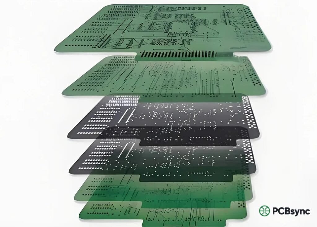
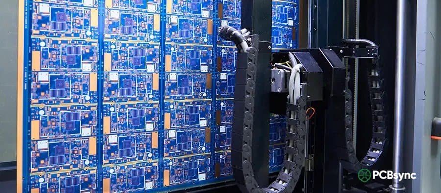
Step 7: Layer Lamination (Multilayer Boards)
For multilayer boards, individual layers must be bonded into a solid stack. This process uses prepreg—partially cured fiberglass cloth impregnated with epoxy resin—as both adhesive and insulating material between copper layers.
The stack-up is carefully arranged: copper foil on the outside, prepreg layers, inner core layers, more prepreg, and finally another copper foil. This sandwich goes into a hydraulic press where heat (typically 180-200°C) and pressure (300-500 PSI) cause the prepreg resin to flow and cure, permanently bonding all layers together.
Lamination parameters—temperature ramp rates, hold times, pressure prof
iles—must be precisely controlled to ensure complete resin flow without compressing features or creating voids. Poor lamination leads to delamination failures in the field.
Step 8: Drilling
Drilling creates holes for component mounting and vias (vertical interconnect access) that connect different layers. Modern CNC drilling machines use carbide or diamond-coated bits spinning at 100,000+ RPM to create holes as small as 0.1mm in diameter.
Registration accuracy is critical. The drilling machine uses X-ray alignment systems to locate inner layer targets and position holes precisely relative to buried features. Even small registration errors cause vias to miss their target pads—a defect called “breakout.”
For HDI boards requiring even smaller holes (microvias below 0.15mm), laser drilling replaces mechanical methods. Laser drills can create blind vias (connecting outer to inner layers) and buried vias (connecting inner layers only) that enable the high-density routing modern electronics demand.
Step 9: Electroless Copper Deposition (Desmear and PTH)
Drilled holes have non-conductive walls—the exposed fiberglass and epoxy of the substrate. To create electrical connections between layers, these hole walls must be made conductive through plated through-hole (PTH) processing.
First, a desmear process removes any resin smeared over copper surfaces during drilling. This ensures good metal-to-metal contact. Then, an electroless copper bath deposits a thin (0.5-1.0 micron) seed layer of copper chemically onto all surfaces, including hole walls. This conductive layer enables subsequent electrolytic plating.
Step 10: Outer Layer Imaging
With holes drilled and plated, the outer layers can now be patterned. The process mirrors inner layer imaging: clean the panel, apply photoresist, expose through film or LDI, and develop to reveal the circuit pattern.
However, outer layer processing uses a negative pattern—the photoresist remains where copper should stay (traces and pads), exposing areas where copper will be removed. This allows for subsequent pattern plating that builds up copper thickness on traces and in holes.
Step 11: Pattern Plating
Electrolytic copper plating builds up additional copper on exposed surfaces—the circuit traces and hole interiors. The panels are immersed in copper sulfate solution while electrical current drives copper ions onto the conductive surfaces.
Plating thickness is carefully controlled, typically adding 20-25 microns of copper to meet minimum conductor thickness requirements. After copper plating, a thin layer of tin or tin-lead is plated over the copper. This tin serves as an etch resist in the next step, protecting the circuit pattern during final etching.
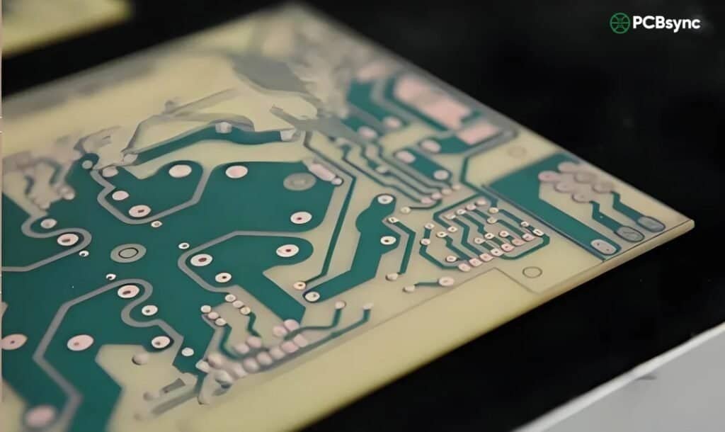
Step 12: Outer Layer Etching
The photoresist is stripped away, exposing the thin electroless copper beneath. This exposed copper is then etched away, but the tin-plated circuit pattern resists the etchant. The result is the final outer layer circuit pattern.
After etching, the protective tin layer is chemically stripped, leaving bare copper traces. At this point, the board has all its circuit patterns complete, but the copper is still exposed and susceptible to oxidation.
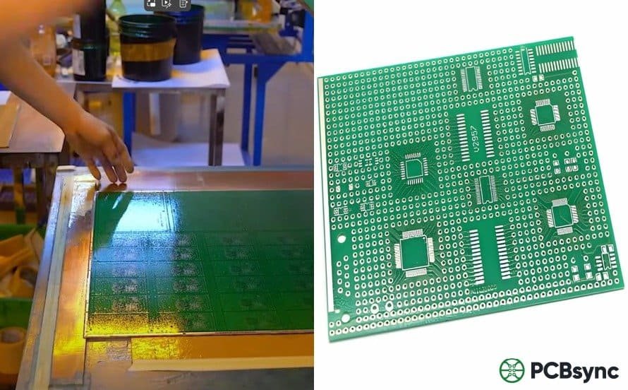
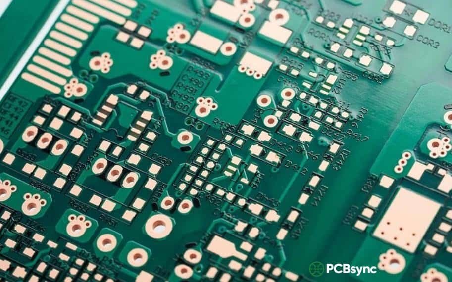
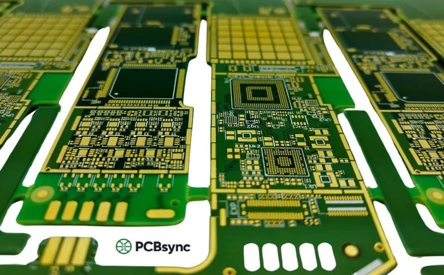
Step 13: Solder Mask Application
The familiar green (or other colored) coating on PCBs is the solder mask—a polymer layer that protects copper traces from oxidation, prevents solder bridges during assembly, and provides electrical insulation.
Liquid photoimageable solder mask (LPISM) is applied by curtain coating or screen printing, then exposed through a film that defines openings for solder pads and vias. Development removes unexposed mask, and thermal curing hardens the remaining polymer. The mask must adhere well, resist soldering temperatures, and provide long-term protection.
Step 14: Surface Finish Application
Exposed copper pads need protection until components are soldered. Various surface finishes serve this purpose, each with distinct characteristics for cost, shelf life, and assembly compatibility.
Finish
Pros
Cons
Best For
HASL
Low cost, excellent solderability, reworkable
Uneven surface, thermal stress
Through-hole, general purpose
ENIG
Flat surface, long shelf life, lead-free
Higher cost, black pad risk
BGA, fine-pitch SMT
OSP
Low cost, flat, eco-friendly
Short shelf life, limited reflows
High-volume SMT assembly
Imm. Silver
Flat, good solderability, RoHS compliant
Tarnishing, handling sensitivity
RF/microwave, membrane switches
Imm. Tin
Very flat, good for press-fit
Tin whiskers, short shelf life
Press-fit connectors, backplanes
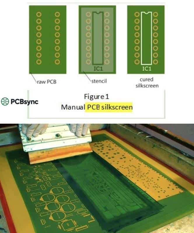
Step 15: Silkscreen and Legend Printing
The silkscreen layer adds human-readable information to the board: component reference designators (R1, C5, U3), polarity markers, logos, version numbers, and other identifying information. This aids assembly operators and technicians during manufacturing and troubleshooting.
Screen printing or inkjet printing applies epoxy-based ink, typically white on green solder mask. The ink must resist soldering temperatures and cleaning chemicals while maintaining legibility throughout the product’s life.
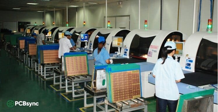
Step 16: Electrical Testing and Final Inspection
Every production board must pass electrical testing before shipment. This verifies that all intended connections exist (continuity) and no unintended connections exist (isolation). Two primary methods accomplish this:
Flying Probe Testing
Moveable probes contact test points sequentially, checking connectivity across the board. This method requires no custom fixture, making it ideal for prototypes and low-volume production. Modern flying probe testers can achieve test pitches as fine as 0.1mm and can also perform capacitance and inductance measurements.
Bed of Nails Testing
A custom fixture with spring-loaded pins contacts all test points simultaneously, enabling rapid testing—often under 30 seconds per board. The upfront fixture cost (thousands of dollars) makes this economical only for high-volume production, but the per-board test time savings are substantial.
After electrical testing, final visual inspection checks for cosmetic defects, proper marking, and overall quality. Boards are then profiled (routed to final shape), cleaned, and prepared for packaging and shipment.
Read more: A Step-by-Step Introduction of PCB Manufacturing :
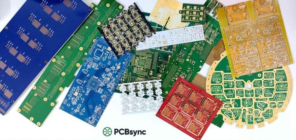
The substrate material significantly impacts a board’s electrical, thermal, and mechanical properties. While FR-4 dominates general-purpose applications, specialized applications demand specialized materials.
Material
Properties
Typical Applications
FR-4
Glass-reinforced epoxy, Tg 130-140°C, low cost
Consumer electronics, general industrial
High-Tg FR-4
Tg 170-180°C, better thermal stability
Lead-free assembly, automotive, servers
Polyimide
Flexible, high temperature resistance, durable
Flex circuits, aerospace, wearables
Rogers/PTFE
Low dielectric loss, controlled Dk, expensive
RF/microwave, 5G, radar systems
Aluminum
Metal core, excellent heat dissipation
LED lighting, power electronics
Quality Standards in PCB Manufacturing
The PCB industry operates under rigorous quality standards, primarily developed by IPC (Association Connecting Electronics Industries). Understanding these standards helps you specify requirements and evaluate manufacturer capabilities.
IPC-A-600: Acceptability of Printed Boards—defines visual quality criteria for bare PCBs
IPC-6012: Qualification and Performance Specification for Rigid Printed Boards—establishes performance classes
IPC-A-610: Acceptability of Electronic Assemblies—covers assembled board quality
J-STD-001: Requirements for Soldered Electrical and Electronic Assemblies
IPC defines three classes based on end-product requirements: Class 1 (General Electronics), Class 2 (Dedicated Service Electronics), and Class 3 (High-Performance Electronics). Specifying the appropriate class ensures your boards meet application requirements without over-engineering.
Useful Resources for PCB Engineers
Here are some valuable resources I’ve found helpful throughout my career for staying current on PCB manufacturing technologies and best practices:
Design Software and Tools
KiCad (kicad.org) – Free, open-source PCB design suite
Altium Designer (altium.com) – Industry-standard professional PCB design
Saturn PCB Toolkit (saturnpcb.com) – Free calculators for trace width, via current, etc.
Standards and Documentation
IPC Standards (ipc.org) – Official source for industry standards
Gerber Format Specification (ucamco.com) – Official Gerber RS-274X documentation
Learning and Community
Rick Hartley’s EMC/Signal Integrity Seminars – Essential for high-speed design
EEVblog Forums (eevblog.com/forum) – Active electronics engineering community
PCB Design Subreddit (reddit.com/r/PCBDesign) – Peer discussions and feedback
Frequently Asked Questions
How long does the PCB manufacturing process take?
Standard turnaround for prototype quantities typically ranges from 5-10 business days for simple 2-layer boards, with multilayer and complex designs taking 2-3 weeks. Quick-turn services can deliver in 24-72 hours for simple boards, but expect premium pricing. Production orders usually require 2-4 weeks depending on volume and complexity.
What’s the difference between PCB fabrication and PCB assembly?
PCB fabrication creates the bare board—the physical structure with copper traces, holes, and protective coatings but no components. PCB assembly (PCBA) is the subsequent process of mounting and soldering electronic components onto the fabricated board. Many manufacturers offer both services, referred to as “turnkey” manufacturing.
What factors most affect PCB manufacturing cost?
The primary cost drivers include layer count (more layers = more processing steps), board size and panelization efficiency, minimum trace/space specifications (finer features require more precise equipment), hole sizes (especially laser-drilled microvias), surface finish selection, and order quantity. Special materials like Rogers laminates also significantly increase cost compared to standard FR-4.
How do I choose between different surface finishes?
Consider your assembly method (through-hole vs. SMT vs. mixed), component types (fine-pitch BGAs need flat surfaces like ENIG), shelf life requirements, environmental regulations (RoHS compliance), and budget. For general-purpose boards with moderate shelf life requirements, lead-free HASL offers good value. For fine-pitch components or extended storage, ENIG is typically preferred despite higher cost.
What file formats do PCB manufacturers need?
A complete manufacturing package typically includes: Gerber RS-274X files for all copper layers, solder mask, and silkscreen; Excellon drill files; a fabrication drawing or README with stackup, materials, and specifications; for assembly, you’ll also need a Bill of Materials (BOM), component placement files (pick-and-place data), and assembly drawings. ODB++ or IPC-2581 formats can consolidate much of this into single intelligent packages.
Conclusion
The PCB manufacturing process represents a remarkable convergence of chemistry, physics, and precision engineering. Each of the 16 steps we’ve covered plays a critical role in transforming your design files into functional circuit boards. Understanding this process doesn’t just satisfy curiosity—it makes you a better designer and a more effective partner for your manufacturing team.
As you work on your next project, keep these manufacturing realities in mind. Design with manufacturability as a priority, communicate early and often with your fabricator, and never underestimate the importance of proper documentation. The boards you design will only be as good as the manufacturing process that produces them—and now you understand exactly what that process entails.
Whether you’re prototyping a hobby project or developing the next generation of mission-critical electronics, the fundamentals of PCB manufacturing remain consistent. Master them, and you’ll consistently produce designs that manufacture smoothly, perform reliably, and meet your project’s requirements the first time.
Inquire: Call 0086-755-23203480, or reach out via the form below/your sales contact to discuss our design, manufacturing, and assembly capabilities.
Quote: Email your PCB files to Sales@pcbsync.com (Preferred for large files) or submit online. We will contact you promptly. Please ensure your email is correct.
Notes: For PCB fabrication, we require PCB design file in Gerber RS-274X format (most preferred), *.PCB/DDB (Protel, inform your program version) format or *.BRD (Eagle) format. For PCB assembly, we require PCB design file in above mentioned format, drilling file and BOM. Click to download BOM template To avoid file missing, please include all files into one folder and compress it into .zip or .rar format.


