Inquire: Call 0086-755-23203480, or reach out via the form below/your sales contact to discuss our design, manufacturing, and assembly capabilities.
Quote: Email your PCB files to Sales@pcbsync.com (Preferred for large files) or submit online. We will contact you promptly. Please ensure your email is correct.
Notes: For PCB fabrication, we require PCB design file in Gerber RS-274X format (most preferred), *.PCB/DDB (Protel, inform your program version) format or *.BRD (Eagle) format. For PCB assembly, we require PCB design file in above mentioned format, drilling file and BOM. Click to download BOM template To avoid file missing, please include all files into one folder and compress it into .zip or .rar format.
Common PCB Manufacturing Defects: How DFM Prevents Costly Errors
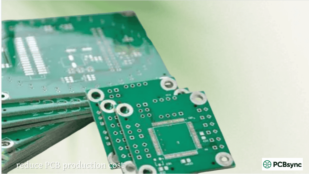
After fifteen years of designing circuit boards, I’ve learned one painful truth: up to 70% of PCB manufacturing issues trace back to design flaws. Every scrapped board, every delayed shipment, every frustrated production manager pointing at yield reports—most of these headaches were preventable during layout. PCB manufacturing defects DFM analysis could have caught them before a single panel was fabricated.
Design for Manufacturability isn’t just another checkbox in your design review process. It’s the difference between boards that glide through production and boards that create expensive bottlenecks. When you understand common manufacturing defects and how they originate in design decisions, you gain the power to eliminate them before they cost real money.
Understanding PCB Manufacturing Defects and Their Impact
Manufacturing defects fall into two broad categories: fabrication defects that occur during bare board production, and assembly defects that happen when components are placed and soldered. Both categories share a common thread—many originate from design decisions made weeks or months before production begins.
The financial impact is significant. A defect caught during design review costs almost nothing to fix. The same defect discovered during fabrication might require a design respin costing thousands. If it escapes to assembly, you’re looking at rework costs, delayed shipments, and potential field failures that damage customer relationships.
The True Cost of PCB Manufacturing Defects
Stage Where Defect Is Caught
Relative Cost to Fix
Impact
Design Review (DFM Check)
1x
Minutes of design time
After Gerber Release
10x
Design respin, schedule delay
During Fabrication
50x
Scrapped panels, expedite fees
During Assembly
100x
Rework, yield loss, line stoppage
Field Failure
1000x+
Warranty costs, reputation damage
This cost multiplier effect explains why PCB manufacturing defects DFM prevention is so critical. Every hour spent on DFM analysis saves days of troubleshooting later.
Common PCB Fabrication Defects
Fabrication defects occur during bare board manufacturing—the etching, drilling, plating, and lamination processes that transform raw materials into circuit boards. Many of these defects have design-related root causes.
Annular Ring Breakout and Insufficient Rings
The annular ring is the copper area surrounding a drilled hole or via. When drill bits wander slightly from their target position—and they always do—insufficient annular rings result in breakout, where the hole partially or completely misses the copper pad.
Why It Happens:
Pad sizes too small for the drill tolerance
High aspect ratio holes with tight tolerances
Drill bit wear causing positional drift
Design doesn’t account for registration tolerances
DFM Prevention: Per IPC-6012 Class 3 requirements, maintain minimum 2 mil annular rings after drilling. For standard production, I recommend designing with at least 4 mil annular rings to accommodate typical manufacturing tolerances. Adding teardrops to trace-pad connections significantly improves reliability when annular rings are marginal.
Acid Traps in Copper Traces
Acid traps form when traces meet at acute angles (less than 90 degrees), creating pockets where etching chemicals become trapped during fabrication. The trapped etchant continues eating away copper long after surrounding areas are clean, resulting in compromised traces or complete opens.
Design Patterns That Create Acid Traps:
Traces meeting at angles less than 90°
Very small gaps between vias and adjacent traces
Complex routing with multiple acute intersections
DFM Prevention: Configure your design rules to flag acute angles. Most EDA tools can enforce minimum angle constraints—I set mine to 90° minimum for standard designs. When acute angles are unavoidable, ensure adequate spacing so etchant can flow freely rather than becoming trapped.
Copper Slivers and Floating Copper
Slivers are thin wedges of copper or solder mask that can detach during fabrication and float to other board areas, causing shorts. They typically form when copper pours create narrow fingers connected to larger areas by thin necks, or when trace spacing creates wedge-shaped gaps.
Sliver Type
Cause
Risk
Conductive (copper)
Thin copper features breaking off
Short circuits between nets
Non-conductive (solder mask)
Narrow mask slivers detaching
Contamination, cosmetic defects
Floating copper
Isolated copper islands
Random shorts, signal integrity issues
DFM Prevention: Set minimum photoresist width rules (typically 3-4 mils minimum). Review copper pours for thin connections and isolated islands. Modern photo-activated etching has reduced sliver issues, but they remain a concern in fine-pitch designs.
Insufficient Drill-to-Copper Clearance
When drilled holes pass too close to copper features on adjacent layers, the risk of shorts increases dramatically. This is particularly problematic in multilayer boards where inner layer copper may not be visible during layout review.
DFM Prevention: Maintain minimum 8 mil drill-to-copper clearance for standard fabrication. This spacing accounts for drill wander, registration tolerances, and plating variations. Run clearance checks on all layers, not just outer layers.
Common PCB Assembly Defects
Assembly defects occur during component placement and soldering. While manufacturing process control plays a major role, many assembly defects have design-related root causes that DFM analysis can identify.
Solder Bridging Between Pads
Solder bridges form unwanted electrical connections between adjacent pads, causing shorts. They’re especially common with fine-pitch components where pad spacing is minimal.
Root Causes:
Excessive solder paste deposition
Pads too close together for stencil aperture design
Missing or insufficient solder mask between pads
Component misalignment during placement
DFM Prevention: Ensure adequate solder mask dams between pads—minimum 4 mil mask width for standard processes. Follow IPC-7351 land pattern guidelines for component footprints. Verify stencil aperture designs account for your paste and reflow profile.
Tombstoning (Manhattan Effect)
Tombstoning occurs when one end of a small passive component lifts off its pad during reflow, leaving the component standing vertically like a tombstone. It happens when surface tension forces on one pad overpower the other during solder melting.
Design Factors Contributing to Tombstoning:
Unequal pad sizes creating thermal imbalance
Different trace widths connecting to each pad
One pad connected to ground plane (heat sink effect)
Component orientation relative to reflow direction
Component Size
Tombstoning Risk
Prevention Strategy
0201
Very High
Matched pads, thermal relief, orientation control
0402
High
Balanced pad design, trace matching
0603
Moderate
Standard thermal relief practices
0805+
Low
Basic DFM sufficient
DFM Prevention: Use symmetrical pad designs with matched trace widths. Apply thermal reliefs to pads connected to copper pours or planes. Orient small passives consistently relative to reflow direction. Consider component placement relative to thermal gradients across the board.
Cold Solder Joints and Poor Wetting
Cold joints occur when solder doesn’t properly wet and bond to both the component lead and PCB pad. They create weak mechanical connections and high-resistance electrical paths that may fail under thermal cycling or vibration.
DFM Prevention: Specify appropriate surface finishes for your assembly process. Ensure pad designs provide adequate solderable area. Avoid contamination risks by specifying proper handling and storage requirements.
Insufficient Solder and Open Joints
Open joints result from inadequate solder volume or poor wetting, leaving no electrical connection between component and pad. They’re often caused by stencil aperture issues or pad design problems.
DFM Prevention: Follow IPC-7351 land pattern recommendations for pad sizing. Ensure stencil designs provide appropriate paste volume for each component type. Review fine-pitch components for adequate paste-to-pad area ratios.
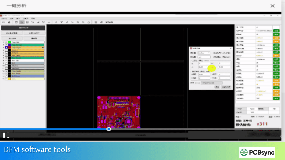
Design for Manufacturability is a systematic approach to identifying and eliminating manufacturing risks during the design phase. It’s distinct from Design Rule Checking (DRC), which only verifies that your design meets predefined spacing and sizing rules.
DFM vs. DRC: Understanding the Difference
Aspect
Design Rule Check (DRC)
Design for Manufacturability (DFM)
Focus
Rule compliance
Actual manufacturability
Scope
Predefined constraints
Manufacturer-specific capabilities
Output
Pass/fail violations
Risk assessment with recommendations
Timing
Throughout design
Before Gerber release
Goal
Design consistency
Production success
DRC tells you if your traces meet minimum spacing rules. DFM tells you if your board will actually yield well in production. Both are essential, but DFM catches issues that pass DRC while still causing manufacturing problems.
Critical DFM Checks for PCB Manufacturing Defects Prevention
A comprehensive PCB manufacturing defects DFM analysis should cover these key areas:
Fabrication Checks:
Minimum trace width and spacing vs. manufacturer capability
Annular ring adequacy for drill tolerances
Drill-to-copper clearance on all layers
Aspect ratio for through-holes and vias
Copper balance for warpage prevention
Acid trap detection at trace intersections
Sliver analysis in copper pours and solder mask
Edge clearance for copper and components
Assembly Checks:
Component-to-component clearance for placement equipment
Component-to-edge clearance for depanelization
Solder mask dam adequacy between fine-pitch pads
Thermal relief design for large pads
Fiducial placement and sizing
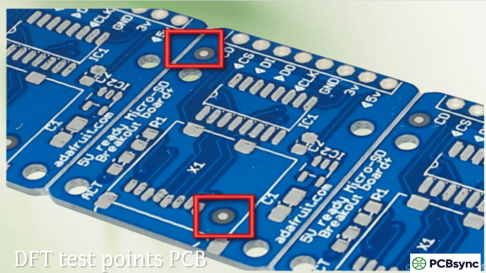
Test point accessibility
Polarity marking visibility
DFM Implementation Best Practices
Start Early: Run preliminary DFM checks during schematic capture when selecting components. Some footprints create inherent manufacturing challenges.
Know Your Manufacturer: Different fabricators have different capabilities. A design that’s easy for one shop might be at the edge of capability for another. Get manufacturer design rules before layout begins.
Iterate Throughout Design: Don’t save DFM for the end. Run checks after major layout milestones to catch issues when they’re easy to fix.
Involve Your CM: Contract manufacturers see thousands of designs. Their engineering teams can identify potential issues you might miss and suggest optimizations based on their specific equipment.
IPC-2221: Generic standard on printed board design
IPC-7351: Generic requirements for surface mount land patterns
IPC-A-610: Acceptability of electronic assemblies
IPC-6012: Qualification and performance specification for rigid PCBs
IPC-2581: Generic requirements for printed board assembly data transfer
Manufacturer Resources
Most PCB fabricators publish design guidelines specific to their capabilities:
Sierra Circuits Design Guide
PCBWay Design Rules
JLCPCB Capabilities
Advanced Circuits Design Resources
Frequently Asked Questions About PCB Manufacturing Defects DFM
What is the difference between DFM and DFA in PCB design?
DFM (Design for Manufacturability) focuses on bare board fabrication—ensuring the PCB itself can be manufactured successfully. It addresses issues like trace spacing, drill sizes, and copper distribution. DFA (Design for Assembly) focuses on component placement and soldering—ensuring components can be reliably placed and soldered to the board. Both are essential; DFM ensures you get good bare boards, while DFA ensures those boards can be successfully assembled into functional products.
How early should DFM analysis start in the design process?
DFM considerations should begin during schematic capture, when you’re selecting components and packages. Some component choices create inherent manufacturing challenges—ultra-fine-pitch BGAs, unusual package types, or components with tight tolerances. Preliminary DFM should run after initial placement, with comprehensive analysis before Gerber release. The earlier you identify issues, the easier and cheaper they are to fix.
Can DFM analysis guarantee zero manufacturing defects?
No analysis can guarantee zero defects—manufacturing involves materials, equipment, and processes that have inherent variability. However, thorough DFM analysis typically improves first-pass yield from 85-90% to 95-99% for complex boards. It eliminates design-related defects, allowing manufacturing teams to focus on process control rather than constantly firefighting design issues. Think of DFM as removing obstacles so manufacturing can perform at its best.
What are the most costly PCB manufacturing defects to fix?
Inner layer defects are typically most costly because they’re difficult to detect and impossible to repair. Annular ring breakout on inner layers, insufficient drill-to-copper clearance causing shorts, and registration errors between layers all require complete board scrapping. Assembly defects like tombstoning or solder bridging can often be reworked, but inner layer fabrication defects mean the entire board is lost.
Should I use my PCB manufacturer’s DFM service or do it myself?
Both approaches have value and ideally you should use both. Running your own DFM analysis during design catches issues early when they’re easiest to fix. Your manufacturer’s DFM analysis validates your design against their specific capabilities and equipment. Some issues that pass generic DFM tools might fail specific manufacturer constraints. Think of internal DFM as development testing and manufacturer DFM as acceptance testing—both are necessary for reliable production.
Building a DFM-First Design Culture
The most effective approach to eliminating PCB manufacturing defects isn’t just running DFM checks—it’s building manufacturability thinking into your entire design process. This means:
Training designers to understand manufacturing processes and how design decisions affect production yield. When engineers understand why certain rules exist, they make better decisions in ambiguous situations.
Establishing relationships with manufacturers early. Bring fabrication and assembly partners into design reviews. Their perspective on what works and what creates problems is invaluable.
Learning from escapes. When defects do occur, trace them back to root causes. Was there a DFM check that could have caught this? Should that check be added to your standard process?
Documenting tribal knowledge. Every organization accumulates hard-won lessons about what works. Capture these in design guidelines that new engineers can follow.
PCB manufacturing defects DFM prevention isn’t about adding bureaucracy to your design process—it’s about front-loading effort to where it creates the most value. An hour of DFM analysis can save days of troubleshooting, thousands in scrapped boards, and immeasurable frustration for everyone in the production chain.
The boards that glide through manufacturing aren’t lucky. They’re designed by engineers who understand that manufacturability is a design requirement, not an afterthought. Every defect you prevent at the design stage is a problem you’ll never have to solve in production.
Inquire: Call 0086-755-23203480, or reach out via the form below/your sales contact to discuss our design, manufacturing, and assembly capabilities.
Quote: Email your PCB files to Sales@pcbsync.com (Preferred for large files) or submit online. We will contact you promptly. Please ensure your email is correct.
Notes: For PCB fabrication, we require PCB design file in Gerber RS-274X format (most preferred), *.PCB/DDB (Protel, inform your program version) format or *.BRD (Eagle) format. For PCB assembly, we require PCB design file in above mentioned format, drilling file and BOM. Click to download BOM template To avoid file missing, please include all files into one folder and compress it into .zip or .rar format.


